- 您现在的位置:买卖IC网 > PDF目录80080 > LT3500IMSE#PBF (LINEAR TECHNOLOGY CORP) 3.5 A SWITCHING REGULATOR, 2800 kHz SWITCHING FREQ-MAX, PDSO16 PDF资料下载
参数资料
| 型号: | LT3500IMSE#PBF |
| 厂商: | LINEAR TECHNOLOGY CORP |
| 元件分类: | 稳压器 |
| 英文描述: | 3.5 A SWITCHING REGULATOR, 2800 kHz SWITCHING FREQ-MAX, PDSO16 |
| 封装: | LEAD FREE, PLASTIC, MSOP-16 |
| 文件页数: | 3/28页 |
| 文件大小: | 318K |
| 代理商: | LT3500IMSE#PBF |
第1页第2页当前第3页第4页第5页第6页第7页第8页第9页第10页第11页第12页第13页第14页第15页第16页第17页第18页第19页第20页第21页第22页第23页第24页第25页第26页第27页第28页
LT3500
11
3500fc
VIN undervoltage detection or thermal shutdown will
set the soft-start latch, resulting in a complete soft-start
sequence.
The switch driver operates from either the VIN or BST volt-
age. An external diode and capacitor are used to generate
a drive voltage higher than VIN to saturate the output NPN
and maintain high efciency.
In addition to the switching regulator, the LT3500 contains
a NPN linear regulator with a 0.8V reference, and 13mA
current capability. The 0.8 reference will track the SS pin
OPERATION
in the same manner as the switching regulator. The linear
output can also be congured to drive an external NPN to
provide a linear regulator with higher current capability.
A power good comparator with 30mV of hysteresis trips
when both FB and LFB are above 90% of the 0.8V refer-
ence. The PG output is an open collector NPN that is off
when the output is in regulation allowing a resistor to pull
the PG pin to a desired voltage. The PG output is an open-
collector NPN that is on when the output is in regulation
providing either drive for an output disconnect transistor
or inverted power good logic.
Choosing the Output Voltage
The output voltage is programmed with a resistor divider
between the output and the FB pin. Choose the 1% resis-
tors according to:
R1
=R2
VOUT1
0.8V
–1
R2 should be 10.0k or less to avoid bias current errors.
Reference designators refer to the Block Diagram in
Figure 1.
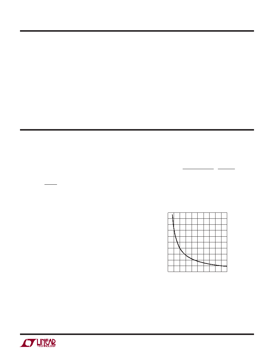
Choosing the Switching Frequency
The LT3500 switching frequency is set by resistor R5 in
Figure 1. The RT/SYNC pin is internally regulated at 1V.
Setting resistor R5 sets the current in the RT/SYNC pin
which determines the oscillator frequency as illustrated
in Figure 2.
The switching frequency is typically set as high as pos-
sible to reduce overall solution size. The LT3500 employs
techniques to enhance dropout at high frequencies but
efciency and maximum input voltage decrease due to
switching losses and minimum switch on times. The
maximum recommended frequency can be approximated
by the equation:
Frequency (Hz)
=
V
OUT1 + VD
V
IN VSW + VD
1
t
ON(MIN)
where VD is the forward voltage drop of the catch diode
(D1 Figure 1), VSW is the voltage drop of the internal
switch, and tON(MIN) is the minimum on time of the
switch, all at maximum load current.
Figure 2. Frequency vs RT/SYNC Resistance
APPLICATIONS INFORMATION
RRT/SYNC (kΩ)
0
FREQUENCY
(kHz) 1500
2000
2500
160
3500 F02
1000
500
1250
1750
2250
750
250
0
40
20
80
60
120 140
180
100
200
相关PDF资料 |
PDF描述 |
|---|---|
| LWN1801-6EM1FK2G | DC-DC REG PWR SUPPLY MODULE |
| LWN1801-6EM2FK2G | DC-DC REG PWR SUPPLY MODULE |
| LT1304CS8-5#PBF | 1.2 A SWITCHING REGULATOR, 300 kHz SWITCHING FREQ-MAX, PDSO8 |
| LX1004CDM-2.5-TR | 1-OUTPUT TWO TERM VOLTAGE REFERENCE, 2.5 V, PDSO8 |
| LT3574EMS#TRPBF | 1.1 A SWITCHING REGULATOR, 1000 kHz SWITCHING FREQ-MAX, PDSO16 |
相关代理商/技术参数 |
参数描述 |
|---|---|
| LT3500IMSE-TRPBF | 制造商:LINER 制造商全称:Linear Technology 功能描述:Monolithic 2A Step-Down Regulator Plus Linear Regulator/Controller |
| LT3500T | 制造商:Eaton Corporation 功能描述:TYPE LT TRIP UNIT ONLY 3P 500A 600VAC MAX |
| LT3501 | 制造商:LINER 制造商全称:Linear Technology 功能描述:Monolithic Dual Tracking 3A Step-Down Switching Regulator |
| LT3501_12 | 制造商:LINER 制造商全称:Linear Technology 功能描述:Monolithic Dual Tracking 3A Step-Down Switching |
| LT3501EFE | 制造商:Linear Technology 功能描述:Conv DC-DC Dual Step Down 3.1V to 25V 20-Pin TSSOP EP |
发布紧急采购,3分钟左右您将得到回复。