- 您现在的位置:买卖IC网 > PDF目录39399 > LT3500IMSE#TRPBF (LINEAR TECHNOLOGY CORP) 3.5 A SWITCHING REGULATOR, 2800 kHz SWITCHING FREQ-MAX, PDSO16 PDF资料下载
参数资料
| 型号: | LT3500IMSE#TRPBF |
| 厂商: | LINEAR TECHNOLOGY CORP |
| 元件分类: | 稳压器 |
| 英文描述: | 3.5 A SWITCHING REGULATOR, 2800 kHz SWITCHING FREQ-MAX, PDSO16 |
| 封装: | LEAD FREE, PLASTIC, MSOP-16 |
| 文件页数: | 9/28页 |
| 文件大小: | 318K |
| 代理商: | LT3500IMSE#TRPBF |
第1页第2页第3页第4页第5页第6页第7页第8页当前第9页第10页第11页第12页第13页第14页第15页第16页第17页第18页第19页第20页第21页第22页第23页第24页第25页第26页第27页第28页
LT3500
17
3500fc
Figure 5. BST Pin Considerations
VBST – VSW = VX
VBST(MAX) = VX
VX > VIN + 3V
(5d)
(5c)
(5b)
VBST – VSW = VIN
VBST(MAX) = 2 VIN
VIN
D2
D1
(5a)
LT3500
LDRV
BST
SW
VBST – VSW = VOUT1
VBST(MAX) = VIN + VOUT1
VBST – VSW = VOUT2
VBST(MAX) = VIN + VOUT2
VOUT2 ≥ 2.5V
VOUT1
VOUT2
C3
VIN
D2
LT3500
LDRV
BST
SW
VOUT1
VIN
LT3500
LDRV
BST
SW
VOUT1
C3
VIN
D2
LT3500
LDRV
BST
SW
D2
VOUT1
C3
3500 F05
The only reason to consider a larger diode is the worst-
case condition of a high input voltage and shorted output.
With a shorted condition, diode current will increase to a
typical value of 3A, determined by the peak switch current
limit of the LT3500. This is safe for short periods of time,
but it would be prudent to check with the diode manu-
facturer if continuous operation under these conditions
can be tolerated.
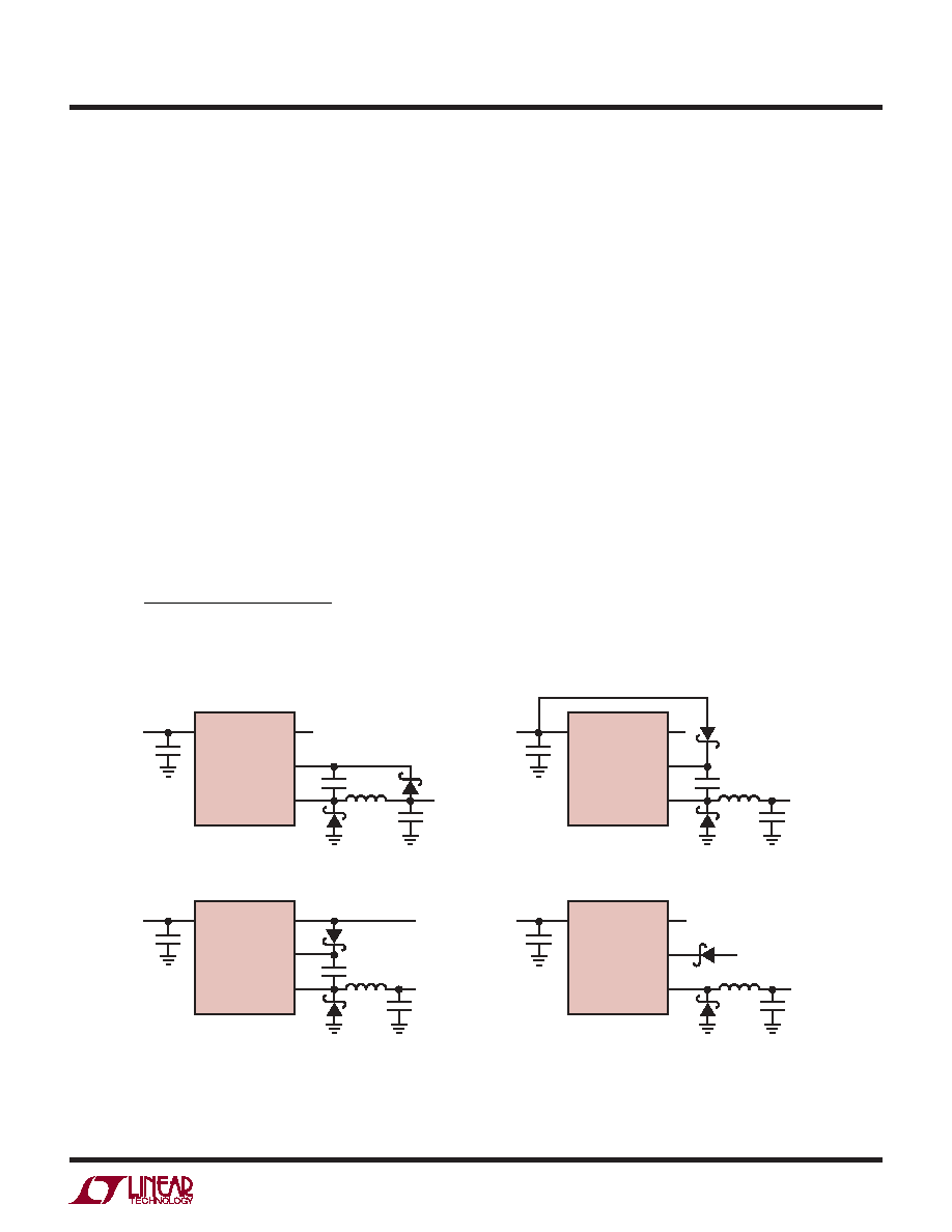
BST Pin Considerations
The capacitor and diode tied to the BST pin generate
a voltage that is higher than the input voltage. In most
cases a 0.47μF capacitor and fast switching diode (such
as the CMDSH-3 or FMMD914) will work well. Almost
any type of lm or ceramic capacitor is suitable, but the
ESR should be <1Ω to ensure it can be fully recharged
during the off time of the switch. The capacitor value can
be approximated by:
C
BST =
I
OUT1(MAX) DC
50 V
OUT1 VBST(MIN)
()f
where IOUT1(MAX) is the maximum load current, and
VBST(MIN) is the minimum boost voltage to fully saturate
the switch.
Figure 5 shows four ways to arrange the boost circuit.
The BST pin must be more than 2.2V above the SW pin
for full efciency.
Generally, for outputs of 3.3V and higher the standard
circuit (Figure 5a) is the best. For outputs between 2.8V
and 3.3V, replace the D2 with a small Schottky diode such
as the PMEG4005.
For lower output voltages the boost diode can be tied to
the input (Figure 5b). The circuit in Figure 5a is more ef-
cient because the BST pin current comes from a lower
voltage source.
Figure 5c shows the boost voltage source from the linear
output that is set to greater than 2.5V (any available DC
sources that are greater than 2.5V is sufcient). The highest
efciency is attained by choosing the lowest boost volt-
age above 2.5V. You must also be sure that the maximum
voltage at the BST pin is less than the maximum specied
in the Absolute Maximum Ratings section.
APPLICATIONS INFORMATION
相关PDF资料 |
PDF描述 |
|---|---|
| LT3757MPMSE#TRPBF | SWITCHING REGULATOR, 1000 kHz SWITCHING FREQ-MAX, PDSO10 |
| LT3757HMSE#TRPBF | SWITCHING REGULATOR, 1000 kHz SWITCHING FREQ-MAX, PDSO10 |
| LT574AKNW | 1-CH 12-BIT SUCCESSIVE APPROXIMATION ADC, PARALLEL ACCESS, PDIP28 |
| LT574ALNW | 1-CH 12-BIT SUCCESSIVE APPROXIMATION ADC, PARALLEL ACCESS, PDIP28 |
| LT574AJNW | 1-CH 12-BIT SUCCESSIVE APPROXIMATION ADC, PARALLEL ACCESS, PDIP28 |
相关代理商/技术参数 |
参数描述 |
|---|---|
| LT3500T | 制造商:Eaton Corporation 功能描述:TYPE LT TRIP UNIT ONLY 3P 500A 600VAC MAX |
| LT3501 | 制造商:LINER 制造商全称:Linear Technology 功能描述:Monolithic Dual Tracking 3A Step-Down Switching Regulator |
| LT3501_12 | 制造商:LINER 制造商全称:Linear Technology 功能描述:Monolithic Dual Tracking 3A Step-Down Switching |
| LT3501EFE | 制造商:Linear Technology 功能描述:Conv DC-DC Dual Step Down 3.1V to 25V 20-Pin TSSOP EP |
| LT3501EFE#PBF | 功能描述:IC REG BUCK ADJ 3A DL 20TSSOP RoHS:是 类别:集成电路 (IC) >> PMIC - 稳压器 - DC DC 开关稳压器 系列:- 标准包装:250 系列:- 类型:降压(降压) 输出类型:固定 输出数:1 输出电压:1.2V 输入电压:2.05 V ~ 6 V PWM 型:电压模式 频率 - 开关:2MHz 电流 - 输出:500mA 同步整流器:是 工作温度:-40°C ~ 85°C 安装类型:表面贴装 封装/外壳:6-UFDFN 包装:带卷 (TR) 供应商设备封装:6-SON(1.45x1) 产品目录页面:1032 (CN2011-ZH PDF) 其它名称:296-25628-2 |
发布紧急采购,3分钟左右您将得到回复。