- 您现在的位置:买卖IC网 > PDF目录98002 > LT3503EDCB (LINEAR TECHNOLOGY CORP) 1 A SWITCHING REGULATOR, 2400 kHz SWITCHING FREQ-MAX, PDSO6 PDF资料下载
参数资料
| 型号: | LT3503EDCB |
| 厂商: | LINEAR TECHNOLOGY CORP |
| 元件分类: | 稳压器 |
| 英文描述: | 1 A SWITCHING REGULATOR, 2400 kHz SWITCHING FREQ-MAX, PDSO6 |
| 封装: | 2 X 3 MM, PLASTIC, MO-229, DFN-6 |
| 文件页数: | 9/20页 |
| 文件大小: | 423K |
| 代理商: | LT3503EDCB |
17
LT3503
3503f
APPLICATIO S I FOR ATIO
WU
U
local, unbroken ground plane below these components,
and tie this ground plane to system ground at one location,
ideally at the ground terminal of the output capacitor C1.
The SW and BOOST nodes should be as small as possible.
Finally, keep the FB node small so that the ground pin and
ground traces will shield it from the SW and BOOST nodes.
Include vias near the exposed GND pad of the LT3503 to
help remove heat from the LT3503 to the ground plane.
High Temperature Considerations
The die temperature of the LT3503 must be lower than the
maximum junction of 125
°C. This is generally not a
concern unless the ambient temperature is above 85
°C.
For higher temperatures, care should be taken in the layout
of the circuit to ensure good heat sinking of the LT3503.
The maximum load current should be derated as the
ambient temperature approaches 125
°C. The die tem-
perature is calculated by multiplying the LT3503 power
dissipation by the thermal resistance from junction to
ambient. Power dissipation within the LT3503 can be
estimated by calculating the total power loss from an
efficiency measurement and subtracting the catch diode
loss. The resulting temperature rise at full load is nearly
independent of input voltage. Thermal resistance depends
on the layout of the circuit board, but 64
°C/W is typical for
the (2mm
× 3mm) DFN (DCB) package.
Outputs Greater Than 6V
For outputs greater than 6V, add a resistor of 1k to 2.5k
across the inductor to damp the discontinuous ringing of
the SW node, preventing unintended SW current.
Other Linear Technology Publications
Application notes AN19, AN35 and AN44 contain more
detailed descriptions and design information for Buck
regulators and other switching regulators. The LT1376
data sheet has a more extensive discussion of output
ripple, loop compensation and stability testing. Design
Note DN100 shows how to generate a bipolar output
supply using a Buck regulator.
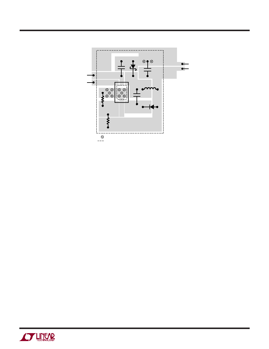
Figure 12. A Good PCB Layout Ensures Proper, Low EMI Operation
C2
D1
C1
SYSTEM
GROUND
: VIAS TO LOCAL GROUND PLANE
: OUTLINE OF LOCAL GROUND PLANE
VOUT
3503 F12
VIN
SHUTDOWN
相关PDF资料 |
PDF描述 |
|---|---|
| LT3585EDDB-2 | 0.95 A BATTERY CHARGE CONTROLLER, PDSO10 |
| LT3585EDDB-0#TRMPDF | 1.3 A BATTERY CHARGE CONTROLLER, PDSO10 |
| LT3585EDDB-3 | 1.85 A BATTERY CHARGE CONTROLLER, PDSO10 |
| LT3587EUD#PBF | SWITCHING REGULATOR, 1200 kHz SWITCHING FREQ-MAX, PQCC20 |
| LT3587EUD#TRPBF | SWITCHING REGULATOR, 1200 kHz SWITCHING FREQ-MAX, PQCC20 |
相关代理商/技术参数 |
参数描述 |
|---|---|
| LT3503EDCB#PBF | 制造商:Linear Technology 功能描述:Conv DC-DC Single Step Down 3.6V to 20V 6-Pin DFN EP 制造商:Linear Technology 功能描述:REG SWITCHING STEP DOWN 1A 2.2MHZ 制造商:Linear Technology 功能描述:REG, SWITCHING, STEP DOWN, 1A 2.2MHZ 制造商:Linear Technology 功能描述:SP-SWREG/Monolithic, Cut Tape 1A, 2.2MHz Buck Regulator ;RoHS Compliant: Yes |
| LT3503EDCB#TR | 制造商:Linear Technology 功能描述:Conv DC-DC Single Step Down 3.6V to 20V 6-Pin DFN EP T/R |
| LT3503EDCB#TRMPBF | 功能描述:IC REG BUCK ADJ 1A 6DFN RoHS:是 类别:集成电路 (IC) >> PMIC - 稳压器 - DC DC 开关稳压器 系列:- 标准包装:250 系列:- 类型:降压(降压) 输出类型:固定 输出数:1 输出电压:1.2V 输入电压:2.05 V ~ 6 V PWM 型:电压模式 频率 - 开关:2MHz 电流 - 输出:500mA 同步整流器:是 工作温度:-40°C ~ 85°C 安装类型:表面贴装 封装/外壳:6-UFDFN 包装:带卷 (TR) 供应商设备封装:6-SON(1.45x1) 产品目录页面:1032 (CN2011-ZH PDF) 其它名称:296-25628-2 |
| LT3503EDCB#TRPBF | 功能描述:IC REG BUCK ADJ 1A 6DFN RoHS:是 类别:集成电路 (IC) >> PMIC - 稳压器 - DC DC 开关稳压器 系列:- 标准包装:2,500 系列:- 类型:升压(升压) 输出类型:可调式 输出数:1 输出电压:1.24 V ~ 30 V 输入电压:1.5 V ~ 12 V PWM 型:电流模式,混合 频率 - 开关:600kHz 电流 - 输出:500mA 同步整流器:无 工作温度:-40°C ~ 85°C 安装类型:表面贴装 封装/外壳:8-SOIC(0.154",3.90mm 宽) 包装:带卷 (TR) 供应商设备封装:8-SOIC |
| LT3503EDCBTRMPBF | 制造商:Linear Technology 功能描述:DC-DC Converter Step-Down 3.6-20V DFN6EP |
发布紧急采购,3分钟左右您将得到回复。