- 您现在的位置:买卖IC网 > PDF目录79747 > LT3506AIDHD#TR (LINEAR TECHNOLOGY CORP) 3.6 A SWITCHING REGULATOR, 1200 kHz SWITCHING FREQ-MAX, PDSO16 PDF资料下载
参数资料
| 型号: | LT3506AIDHD#TR |
| 厂商: | LINEAR TECHNOLOGY CORP |
| 元件分类: | 稳压器 |
| 英文描述: | 3.6 A SWITCHING REGULATOR, 1200 kHz SWITCHING FREQ-MAX, PDSO16 |
| 封装: | 5 X 4 MM, PLASTIC, MO-229WJGD-2, DFN-16 |
| 文件页数: | 4/24页 |
| 文件大小: | 210K |
| 代理商: | LT3506AIDHD#TR |
LT3506/LT3506A
12
3506afc
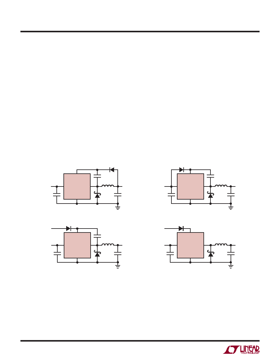
BOOST Pin Considerations
The capacitor and diode tied to the BOOST pin generate
a voltage that is higher than the input voltage. In most
cases a 0.1μF capacitor and fast switching diode (such
as the CMDSH-3 or FMMD914) will work well. Figure 3
shows three ways to arrange the boost circuit. The BOOST
pin must be more than 2.5V above the SW pin for full
efciency. For outputs of 3.3V and higher the standard
circuit (Figure 3a) is best. For outputs between 2.8V and
3.3V, use a small Schottky diode (such as the BAT-54).
For lower output voltages the boost diode can be tied to
the input (Figure 3b). The circuit in Figure 3a is more ef-
cient because the BOOST pin current comes from a lower
voltage source. Finally, as shown in Figure 3c, the anode
of the boost diode can be tied to another source that is
at least 3V. For example, if you are generating 3.3V and
1.8V and the 3.3V is on whenever the 1.8V is on, the 1.8V
boost diode can be connected to the 3.3V output. In any
case, you must also be sure that the maximum voltage at
the BOOST pin is less than the maximum specied in the
Absolute Maximum Ratings section.
The boost circuit can also run directly from a DC voltage
that is higher than the input voltage by more than 3V,
as in Figure 3d. The diode is used to prevent damage to
the LT3506 in case VINB is held low while VIN is present.
The circuit saves several components (both BOOST pins
can be tied to D2). However, efciency may be lower and
dissipation in the LT3506 may be higher. Also, if VINB is
absent, the LT3506 will still attempt to regulate the output,
but will do so with very low efciency and high dissipation
because the switch will not be able to saturate, dropping
1.5V to 2V in conduction.
VIN
BOOST
GND
SW
VIN
LT3506
(3a)
D2
VOUT
C3
VBOOST – VSW VOUT
MAX VBOOST VIN + VOUT
VIN
BOOST
GND
SW
VIN
LT3506
(3b)
D2
VOUT
C3
VBOOST – VSW VIN
MAX VBOOST 2VIN
VIN
BOOST
GND
SW
VIN
LT3506
(3d)
3506 F03
VOUT
MAX VBOOST – VSW VINB
MAX VBOOST VINB
MINIMUM VALUE FOR VINB = VIN + 3V
VINB
>VIN + 3V
D2
VIN
BOOST
GND
SW
VIN
LT3506
(3c)
VOUT
VBOOST – VSW VINB
MAX VBOOST VINB + VIN
MINIMUM VALUE FOR VINB = 3V
D2
VINB > 3V
C3
Figure 3. Generating the Boost Voltage
APPLICATIONS INFORMATION
相关PDF资料 |
PDF描述 |
|---|---|
| LT1460DCS8-10#TR1460 | 1-OUTPUT THREE TERM VOLTAGE REFERENCE, 10 V, PDSO8 |
| LT1460FCMS8-5#PBF1460 | 1-OUTPUT THREE TERM VOLTAGE REFERENCE, 5 V, PDSO8 |
| LM4040DIZ-2.0/NOPB | 1-OUTPUT TWO TERM VOLTAGE REFERENCE, 2.048 V, PBCY3 |
| LTC692IN8#PBF | 1-CHANNEL POWER SUPPLY SUPPORT CKT, PDIP8 |
| LT1009CDRE4 | 1-OUTPUT TWO TERM VOLTAGE REFERENCE, 2.5 V, PDSO8 |
相关代理商/技术参数 |
参数描述 |
|---|---|
| LT3506AIDHD-TRPBF | 制造商:LINER 制造商全称:Linear Technology 功能描述:Dual Monolithic 1.6A Step-Down Switching Regulator |
| LT3506AIFE | 制造商:LINER 制造商全称:Linear Technology 功能描述:Dual Monolithic 1.6A Step-Down Switching Regulator |
| LT3506AIFE#PBF | 功能描述:IC REG BUCK ADJ 1.6A DL 16TSSOP RoHS:是 类别:集成电路 (IC) >> PMIC - 稳压器 - DC DC 开关稳压器 系列:- 设计资源:Design Support Tool 标准包装:1 系列:- 类型:升压(升压) 输出类型:固定 输出数:1 输出电压:3V 输入电压:0.75 V ~ 2 V PWM 型:- 频率 - 开关:- 电流 - 输出:100mA 同步整流器:是 工作温度:-40°C ~ 85°C 安装类型:表面贴装 封装/外壳:SOT-23-5 细型,TSOT-23-5 包装:剪切带 (CT) 供应商设备封装:TSOT-23-5 其它名称:AS1323-BTTT-30CT |
| LT3506AIFE#TRPBF | 功能描述:IC REG BUCK ADJ 1.6A DL 16TSSOP RoHS:是 类别:集成电路 (IC) >> PMIC - 稳压器 - DC DC 开关稳压器 系列:- 设计资源:Design Support Tool 标准包装:1 系列:- 类型:升压(升压) 输出类型:固定 输出数:1 输出电压:3V 输入电压:0.75 V ~ 2 V PWM 型:- 频率 - 开关:- 电流 - 输出:100mA 同步整流器:是 工作温度:-40°C ~ 85°C 安装类型:表面贴装 封装/外壳:SOT-23-5 细型,TSOT-23-5 包装:剪切带 (CT) 供应商设备封装:TSOT-23-5 其它名称:AS1323-BTTT-30CT |
| LT3506AIFE-PBF | 制造商:LINER 制造商全称:Linear Technology 功能描述:Dual Monolithic 1.6A Step-Down Switching Regulator |
发布紧急采购,3分钟左右您将得到回复。