- 您现在的位置:买卖IC网 > PDF目录80280 > LT3507AIUHF#PBF (LINEAR TECHNOLOGY CORP) SWITCHING REGULATOR, PQCC38 PDF资料下载
参数资料
| 型号: | LT3507AIUHF#PBF |
| 厂商: | LINEAR TECHNOLOGY CORP |
| 元件分类: | 稳压器 |
| 英文描述: | SWITCHING REGULATOR, PQCC38 |
| 封装: | 5 X 7 MM, LEAD FREE, PLASTIC, QFN-38 |
| 文件页数: | 15/28页 |
| 文件大小: | 372K |
| 代理商: | LT3507AIUHF#PBF |
第1页第2页第3页第4页第5页第6页第7页第8页第9页第10页第11页第12页第13页第14页当前第15页第16页第17页第18页第19页第20页第21页第22页第23页第24页第25页第26页第27页第28页

LT3507A
22
3507af
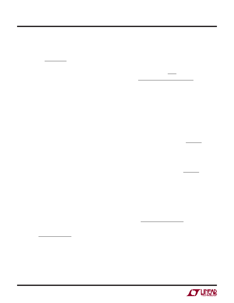
The maximum allowed power dissipation by the LT3507A
can be determined by:
PDISS(MAX) =
TJ(MAX) – TA
θJA
where TJMAX is the maximum die temperature of 125°C
(150°C for H-grade).
However, take care in determining TA since the catch
diodes also dissipate power and must be located close
to the LT3507A. Another potential heat source is the LDO
pass transistor. In a compact layout the pass transistor
will be located close to the LT3507A. The inductors will
also dissipate some power due to their series resistance
and they must be close to the LT3507A. All of these heat
sources will increase the effective ambient temperature
seen by the LT3507A.
A thorough analysis of eight heat sources in a small PCB
area is beyond the scope of this data sheet, however a
number of thermal analysis programs are available to
calculate the temperature rise in each component (such as
PCAnalyze from K&K Associates or Flo Therm PCB from
Mentor). The power dissipation of each component will be
needed to accurately calculate the thermal characteristics
of the system.
The contributors to power dissipation inside the LT3507A
are switch DC loss, switch AC loss, boost current, quies-
cent current and LDO drive current. The total dissipation
within the LT3507A can be expressed as:
PDISS =
PSWDCi +PSWACi +PBSTi
(
)+PQ +PLDO
i
=1
3
∑
The switch DC and AC losses in channel i are:
PSWDCi =
RSWi IOUTi
( )2 VOUTi
VINi
PSWACi =17ns IOUTi
( ) VINi
( ) f()
APPLICATIONS INFORMATION
where RSWi is the equivalent switch resistance (0.18Ω for
channel 1 and 0.22Ω for channels 2 and 3) and f is the
operating frequency.
The boost loss in channel i is:
PBSTi =
VOUTi VBOOSTi
(
) IOUTi
50
+ 0.02A
VINi
The quiescent loss is:
PQ = VIN1(IQ(VIN1)) + VBIAS(IQ(BIAS))
If the BIAS pin does not have a voltage of at least 3V ap-
plied, then VIN1 must replace VBIAS in the equation. Also,
IQ(VIN1) can be reduced by 0.2mA (typ) if the LDO is shut
off (see the LDO section).
The LDO drive loss is:
PLDO =(VBIAS VLDO(OUT) 0.7V)
IOUT(LDO)
βPASS
,
if VBIAS ≥ VLDO(OUT) +1.5V
or
PLDO =(VIN1VLDO(OUT) 0.7V)
IOUT(LDO)
βPASS
,
if VBIAS <VLDO(OUT) +1.5V
where
βPASS is the current gain of the external pass
transistor.
Next, the power in the external components must be taken
into account. The diode power is given by:
PDIODE =
VF VIN – VOUT – VF
(
)IOUT
VIN
where VF is the forward drop of the diode at IOUT.
The inductor power is:
PIND = (IOUT)2 ESRIND
where ESRIND is the inductor equivalent series resistance.
相关PDF资料 |
PDF描述 |
|---|---|
| LS1001-7ERD2B1 | 1-OUTPUT AC-DC REG PWR SUPPLY MODULE |
| LS1001-7ERV0B1 | 1-OUTPUT AC-DC REG PWR SUPPLY MODULE |
| LS1001-7PD7B1 | 1-OUTPUT AC-DC REG PWR SUPPLY MODULE |
| LS1001-7PD9T | 1-OUTPUT AC-DC REG PWR SUPPLY MODULE |
| LS1001-9PDDTB1 | 1-OUTPUT AC-DC REG PWR SUPPLY MODULE |
相关代理商/技术参数 |
参数描述 |
|---|---|
| LT3507EUHF#2ESPBF | 制造商:Linear Technology 功能描述:TRIPLE MONOLITHIC STEP-DOWN REGULATOR WITH LDO |
| LT3507EUHF#PBF | 功能描述:IC REG QD BUCK/LINEAR 38-QFN RoHS:是 类别:集成电路 (IC) >> PMIC - 稳压器 - 线性 + 切换式 系列:- 标准包装:2,500 系列:- 拓扑:降压(降压)同步(3),线性(LDO)(2) 功能:任何功能 输出数:5 频率 - 开关:300kHz 电压/电流 - 输出 1:控制器 电压/电流 - 输出 2:控制器 电压/电流 - 输出 3:控制器 带 LED 驱动器:无 带监控器:无 带序列发生器:是 电源电压:5.6 V ~ 24 V 工作温度:-40°C ~ 85°C 安装类型:* 封装/外壳:* 供应商设备封装:* 包装:* |
| LT3507EUHF#TRPBF | 功能描述:IC REG QD BUCK/LINEAR 38-QFN RoHS:是 类别:集成电路 (IC) >> PMIC - 稳压器 - 线性 + 切换式 系列:- 标准包装:2,500 系列:- 拓扑:降压(降压)同步(3),线性(LDO)(2) 功能:任何功能 输出数:5 频率 - 开关:300kHz 电压/电流 - 输出 1:控制器 电压/电流 - 输出 2:控制器 电压/电流 - 输出 3:控制器 带 LED 驱动器:无 带监控器:无 带序列发生器:是 电源电压:5.6 V ~ 24 V 工作温度:-40°C ~ 85°C 安装类型:* 封装/外壳:* 供应商设备封装:* 包装:* |
| LT3507EUHFPBF | 制造商:Linear Technology 功能描述:Step Down Regulator with LDO |
| LT3507EUHF-PBF | 制造商:LINER 制造商全称:Linear Technology 功能描述:Triple Monolithic Step-Down Regulator with LDO |
发布紧急采购,3分钟左右您将得到回复。