- 您现在的位置:买卖IC网 > PDF目录20871 > LT3519IMS-1#TRPBF (Linear Technology)LED DRIVER WITH INTEGRATED SCHOT PDF资料下载
参数资料
| 型号: | LT3519IMS-1#TRPBF |
| 厂商: | Linear Technology |
| 文件页数: | 12/20页 |
| 文件大小: | 0K |
| 描述: | LED DRIVER WITH INTEGRATED SCHOT |
| 标准包装: | 2,500 |
| 恒定电流: | 是 |
| 恒定电压: | 是 |
| 拓扑: | PWM,SEPIC,降压(降压),升压(升压) |
| 输出数: | 1 |
| 内部驱动器: | 是 |
| 类型 - 主要: | 车载 |
| 频率: | 800kHz ~ 1.1MHz |
| 电源电压: | 3 V ~ 30 V |
| 安装类型: | 表面贴装 |
| 封装/外壳: | 16-TFSOP(0.118",3.00mm 宽) |
| 供应商设备封装: | 16-MSOP |
| 包装: | 带卷 (TR) |
| 工作温度: | -40°C ~ 125°C |
�� �
�
�LT3519/LT3519-1/LT3519-2�
�APPLICATIONS� INFORMATION�
�Open� LED� Detection�
�The� LT3519/LT3519-1/LT3519-2� provide� an� open-collector�
�status� pin,� OPENLED� ,� that� pulls� low� when� the� FB� pin� is�
�within� ~60mV� of� its� 1.22V� regulated� voltage.� If� the� open�
�LED� clamp� voltage� is� programmed� correctly� using� the� FB�
�pin,� then� the� FB� pin� should� never� exceed� 1.1V� when� LEDs�
�are� connected,� therefore,� the� only� way� for� the� FB� pin� to�
�be� within� 60mV� of� the� 1.22V� regulation� voltage� is� for� an�
�open� LED� event� to� have� occurred.�
�Inrush� Current�
�The� LT3519/LT3519-1/LT3519-2� have� a� built-in� Schottky�
�diode� for� a� boost� converter.� When� supply� voltage� is� ap-�
�plied� to� V� IN� pin,� the� voltage� difference� between� V� IN� and�
�V� OUT� generates� inrush� current� ?owing� from� input� through�
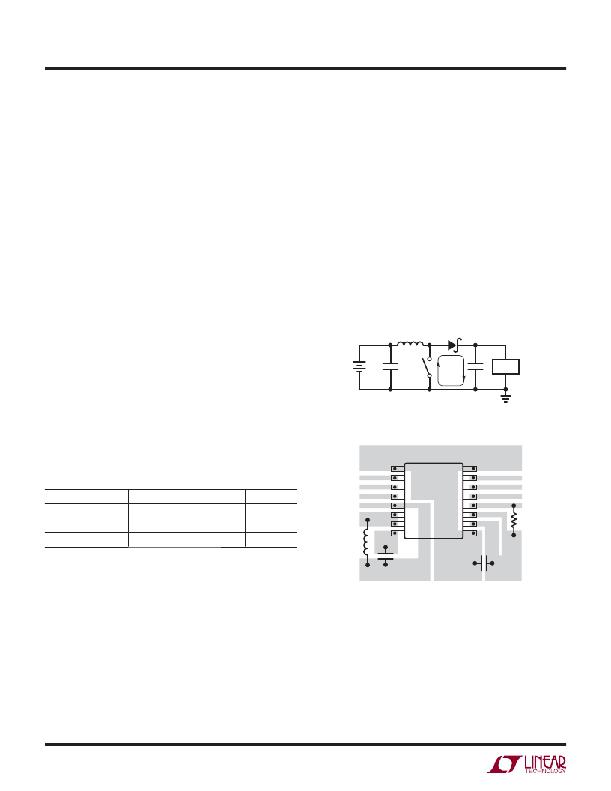
�Board� Layout�
�As� with� all� switching� regulators,� careful� attention� must� be�
�paid� to� the� PCB� board� layout� and� component� placement.�
�To� prevent� electromagnetic� interference� (EMI)� problems,�
�proper� layout� of� high� frequency� switching� paths� (see�
�Figure� 4)� is� essential.� Minimize� the� length� and� area� of� all�
�traces� connected� to� the� switching� node� pin� (SW).� Keep� the�
�sense� voltage� pins� (ISP� and� ISN)� away� from� the� switching�
�node.� The� bypass� capacitor� on� the� V� IN� supply� to� the� LT3519�
�should� be� placed� as� close� as� possible� to� the� V� IN� pin� and�
�GND.� Likewise,� place� C� OUT� next� to� the� CATHODE� pin.� Do�
�not� extensively� route� high� impedance� signals� such� as� FB�
�and� CTRL,� as� they� may� pick� up� switching� noise.� Figure� 5�
�shows� the� recommended� component� placement.�
�the� inductor� and� the� Schottky� diode� to� charge� the� output�
�capacitor.� The� selection� of� inductor� and� capacitor� value�
�should� ensure� the� peak� of� the� inrush� current� to� below�
�+�
�V� IN�
�L1�
�SW�
�D1�
�V� OUT�
�LOAD�
�10A.� In� addition,� the� LT3519/LT3519-1/LT3519-2� turn-on�
�should� be� delayed� until� the� inrush� current� is� less� than� the�
�maximum� current� limit.� If� the� peak� of� the� inrush� current�
�is� more� than� 10A,� an� external� Schottky� diode� should� be�
�used� to� bypass� both� the� inductor� and� internal� Schottky.�
�The� recommended� Schottky� diodes� for� hot� plug� are� shown�
�Figure� 4.� High� Frequency� Path�
�3519� F04�
�on� Table� 3.�
�Table� 3.� Schottky� Diodes� Recommended� for� Hot� Plug�
�GND�
�OPENLED�
�PWM�
�GND�
�V� REF�
�CTRL�
�VENDOR�
�PART� NUMBER�
�V� R� (V)�
�I� AVE� (A)�
�SHDN� /UVLO�
�FB�
�Diodes,� Inc�
�Zetex�
�DFLS160�
�ZLLS10000TA�
�60�
�40�
�1�
�1�
�V� IN� ISN�
�SW� ISP�
�ANODE� CATHODE�
�R� S�
�International� Recti?er�
�10MQ060N�
�60�
�1.5�
�L1�
�GND�
�GND�
�C� IN�
�C� OUT�
�V� IN�
�GND�
�V� OUT�
�3519� F05�
�Figure� 5.� Suggested� Layout�
�3519fa�
�12�
�相关PDF资料 |
PDF描述 |
|---|---|
| EBM10DRXS | CONN EDGECARD 20POS DIP .156 SLD |
| P51-500-S-J-MD-4.5V-000-000 | SENSOR 500PSI 3/8-24 UNF .5-4.5V |
| REC3-4812DRWZ/H6/C/SMD | CONV DC/DC 3W 18-72VIN +/-12VOUT |
| P51-300-A-M-M12-4.5OVP-000-000 | SENSOR 300PSI M10-1.0 6G .5-4.5V |
| P51-300-S-J-MD-4.5V-000-000 | SENSOR 300PSI 3/8-24 UNF .5-4.5V |
相关代理商/技术参数 |
参数描述 |
|---|---|
| LT3519IMS-2#PBF | 功能描述:IC LED DVR W/SCHOTTKY DIO 16MSOP RoHS:是 类别:集成电路 (IC) >> PMIC - LED 驱动器 系列:- 标准包装:6,000 系列:- 恒定电流:- 恒定电压:- 拓扑:开路漏极,PWM 输出数:4 内部驱动器:是 类型 - 主要:LED 闪烁器 类型 - 次要:- 频率:400kHz 电源电压:2.3 V ~ 5.5 V 输出电压:- 安装类型:表面贴装 封装/外壳:8-VFDFN 裸露焊盘 供应商设备封装:8-HVSON 包装:带卷 (TR) 工作温度:-40°C ~ 85°C 其它名称:935286881118PCA9553TK/02-TPCA9553TK/02-T-ND |
| LT3519IMS-2#TRPBF | 功能描述:IC LED DVR W/DIO 2.2MHZ 16MSOP RoHS:是 类别:集成电路 (IC) >> PMIC - LED 驱动器 系列:- 标准包装:6,000 系列:- 恒定电流:- 恒定电压:- 拓扑:开路漏极,PWM 输出数:4 内部驱动器:是 类型 - 主要:LED 闪烁器 类型 - 次要:- 频率:400kHz 电源电压:2.3 V ~ 5.5 V 输出电压:- 安装类型:表面贴装 封装/外壳:8-VFDFN 裸露焊盘 供应商设备封装:8-HVSON 包装:带卷 (TR) 工作温度:-40°C ~ 85°C 其它名称:935286881118PCA9553TK/02-TPCA9553TK/02-T-ND |
| LT3519IMSPBF | 制造商:LINER 制造商全称:Linear Technology 功能描述:LED Driver with Integrated Schottky Diode |
| LT3519IMSTRPBF | 制造商:LINER 制造商全称:Linear Technology 功能描述:LED Driver with Integrated Schottky Diode |
| LT3524 | 制造商:LINER 制造商全称:Linear Technology 功能描述:Regulating Pulse Width Modulator |
发布紧急采购,3分钟左右您将得到回复。