- 您现在的位置:买卖IC网 > PDF目录14841 > LT3580EMS8E#PBF (Linear Technology)IC REG BOOST INV SEPIC 2A 8MSOP PDF资料下载
参数资料
| 型号: | LT3580EMS8E#PBF |
| 厂商: | Linear Technology |
| 文件页数: | 16/28页 |
| 文件大小: | 0K |
| 描述: | IC REG BOOST INV SEPIC 2A 8MSOP |
| 标准包装: | 50 |
| 类型: | 升压(升压),反相,Sepic |
| 输出数: | 1 |
| 输入电压: | 2.5 V ~ 32 V |
| PWM 型: | 电流模式 |
| 频率 - 开关: | 200kHz ~ 2.5MHz |
| 电流 - 输出: | 2A |
| 同步整流器: | 无 |
| 工作温度: | -40°C ~ 125°C |
| 安装类型: | 表面贴装 |
| 封装/外壳: | 8-TSSOP,8-MSOP(0.118",3.00mm 宽)裸露焊盘 |
| 包装: | 管件 |
| 供应商设备封装: | 8-MSOP-EP |
| 产品目录页面: | 1332 (CN2011-ZH PDF) |
第1页第2页第3页第4页第5页第6页第7页第8页第9页第10页第11页第12页第13页第14页第15页当前第16页第17页第18页第19页第20页第21页第22页第23页第24页第25页第26页第27页第28页
�� �
�
�LT3580�
�APPLICATIONS� INFORMATION�
�Board� layout� also� has� a� significant� effect� on� thermal� re-�
�sistance.� The� exposed� package� ground� pad� is� the� copper�
�plate� that� runs� under� the� LT3580� die.� This� is� a� good� thermal�
�path� for� heat� out� of� the� package.� Soldering� the� pad� onto�
�the� board� reduces� die� temperature� and� increases� the� power�
�capability� of� the� LT3580.� Provide� as� much� copper� area� as�
�possible� around� this� pad.� Adding� multiple� feedthroughs�
�around� the� pad� to� the� ground� plane� will� also� help.� Figures�
�9� and� 10� show� the� recommended� component� placement�
�for� the� boost� and� SEPIC� configurations,� respectively.�
�Layout� Hints� for� Inverting� Topology�
�Figure� 11� shows� recommended� component� placement� for�
�the� dual� inductor� inverting� topology.� Input� bypass� capaci-�
�tor,� C1,� should� be� placed� close� to� the� LT3580,� as� shown.�
�The� load� should� connect� directly� to� the� output� capacitor,�
�L1�
�C1�
�C2,� for� best� load� regulation.� You� can� tie� the� local� ground�
�into� the� system� ground� plane� at� the� C3� ground� terminal.�
�The� cut� ground� copper� at� D1’s� cathode� is� essential� to�
�obtain� low� noise.� This� important� layout� issue� arises� due�
�to� the� chopped� nature� of� the� currents� flowing� in� Q1� and�
�D1.� If� they� are� both� tied� directly� to� the� ground� plane� before�
�being� combined,� switching� noise� will� be� introduced� into�
�the� ground� plane.� It� is� almost� impossible� to� get� rid� of� this�
�noise,� once� present� in� the� ground� plane.� The� solution�
�is� to� tie� D1’s� cathode� to� the� ground� pin� of� the� LT3580�
�before� the� combined� currents� are� dumped� in� the� ground�
�plane� as� drawn� in� Figure� 2,� Figure� 12� and� Figure� 13.� This�
�single� layout� technique� can� virtually� eliminate� high�
�frequency� “spike”� noise,� so� often� present� on� switching�
�regulator� outputs.�
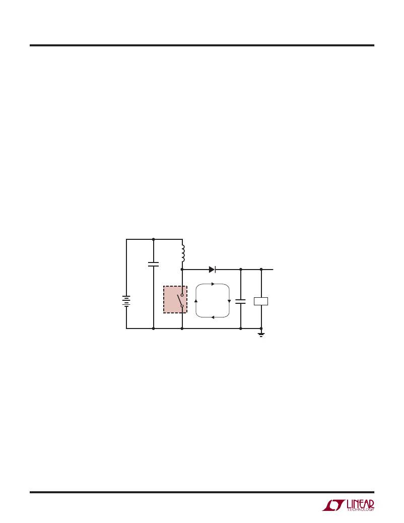
�D1�
�V� OUT�
�SW�
�LT3580�
�HIGH�
�V� IN�
�FREQUENCY�
�SWITCHING�
�C2� LOAD�
�PATH�
�GND�
�3580� F08�
�Figure� 8.� High� Speed� “Chopped”� Switching� Path� for� Boost� Topology�
�3580fg�
�16�
�相关PDF资料 |
PDF描述 |
|---|---|
| ECC19DREH-S734 | CONN EDGECARD 38POS .100 EYELET |
| LT1610CMS8#PBF | IC REG BOOST ADJ 0.6A 8MSOP |
| LTC1682IS8-5#PBF | IC REG MULTI CONFIG 5V 8SOIC |
| MAX6463UK34+T | IC VOLT DETECTOR LP SOT23-5 |
| LT1307CS8#PBF | IC REG BOOST 3.3V/5V 0.1A 8SOIC |
相关代理商/技术参数 |
参数描述 |
|---|---|
| LT3580EMS8E-TRPBF | 制造商:LINER 制造商全称:Linear Technology 功能描述:Boost/Inverting DC/DC Converter with 2A Switch, Soft-Start, and Synchronization |
| LT3580HMS8E | 制造商:LINER 制造商全称:Linear Technology 功能描述:Boost/Inverting DC/DC Converter with 2A Switch, Soft-Start, and Synchronization |
| LT3580HMS8E#PBF | 功能描述:IC REG BOOST INV SEPIC 2A 8MSOP RoHS:是 类别:集成电路 (IC) >> PMIC - 稳压器 - DC DC 开关稳压器 系列:- 标准包装:2,500 系列:- 类型:降压(降压) 输出类型:固定 输出数:1 输出电压:1.2V,1.5V,1.8V,2.5V 输入电压:2.7 V ~ 20 V PWM 型:- 频率 - 开关:- 电流 - 输出:50mA 同步整流器:是 工作温度:-40°C ~ 125°C 安装类型:表面贴装 封装/外壳:10-TFSOP,10-MSOP(0.118",3.00mm 宽)裸露焊盘 包装:带卷 (TR) 供应商设备封装:10-MSOP 裸露焊盘 |
| LT3580HMS8E#TRPBF | 功能描述:IC REG BOOST INV SEPIC 2A 8MSOP RoHS:是 类别:集成电路 (IC) >> PMIC - 稳压器 - DC DC 开关稳压器 系列:- 标准包装:2,500 系列:- 类型:降压(降压) 输出类型:固定 输出数:1 输出电压:1.2V,1.5V,1.8V,2.5V 输入电压:2.7 V ~ 20 V PWM 型:- 频率 - 开关:- 电流 - 输出:50mA 同步整流器:是 工作温度:-40°C ~ 125°C 安装类型:表面贴装 封装/外壳:10-TFSOP,10-MSOP(0.118",3.00mm 宽)裸露焊盘 包装:带卷 (TR) 供应商设备封装:10-MSOP 裸露焊盘 |
| LT3580IDD | 制造商:Linear Technology 功能描述:Conv DC-DC Single Inv/Step Up 2.5V to 32V 8-Pin DFN EP |
发布紧急采购,3分钟左右您将得到回复。