- 您现在的位置:买卖IC网 > PDF目录80141 > LT3652HVIMSE#PBF (LINEAR TECHNOLOGY CORP) BATTERY CHARGE CONTROLLER, PDSO12 PDF资料下载
参数资料
| 型号: | LT3652HVIMSE#PBF |
| 厂商: | LINEAR TECHNOLOGY CORP |
| 元件分类: | 稳压器 |
| 英文描述: | BATTERY CHARGE CONTROLLER, PDSO12 |
| 封装: | LEAD FREE, PLASTIC, MSOP-12 |
| 文件页数: | 4/24页 |
| 文件大小: | 250K |
| 代理商: | LT3652HVIMSE#PBF |
LT3652HV
12
3652hvf
Bulk capacitance is a function of desired input ripple volt-
age (ΔVIN), and follows the relation:
CIN(BULK) = ICHG(MAX) (VBAT/VIN) / ΔVIN (μF)
Input ripple voltages above 0.1V are not recommended.
10μF is typically adequate for most charger applica-
tions.
Charge Current Programming
The LT3652HV charger is configurable to charge at aver-
age currents as high as 2A. Maximum charge current is
set by choosing an inductor sense resistor (RSENSE) such
that the desired maximum average current through that
sense resistor creates a 100mV drop, or:
RSENSE = 0.1 / ICHG(MAX)
where ICHG(MAX) is the maximum average charge current.
A 2A charger, for example, would use a 0.05Ω sense
resistor.
BOOST Supply
The BOOST bootstrapped supply rail drives the internal
switch and facilitates saturation of the switch transistor.
Operating range of the BOOST pin is 0V to 8.5V, as refer-
enced to the SW pin. Connect a 1μF or greater capacitor
from the BOOST pin to the SW pin.
The voltage on the decoupling capacitor is refreshed
through a diode, with the anode connected to either the
battery output voltage or an external source, and the
cathode connected to the BOOST pin. Rate the diode
average current greater than 0.1A, and reverse voltage
greater than VIN(MAX).
To refresh the decoupling capacitor with a rectifying diode
from the battery with battery float voltages higher than
8.4V, a >100mA Zener diode can be put in series with
the rectifying diode to prevent exceeding the BOOST pin
operating voltage range.
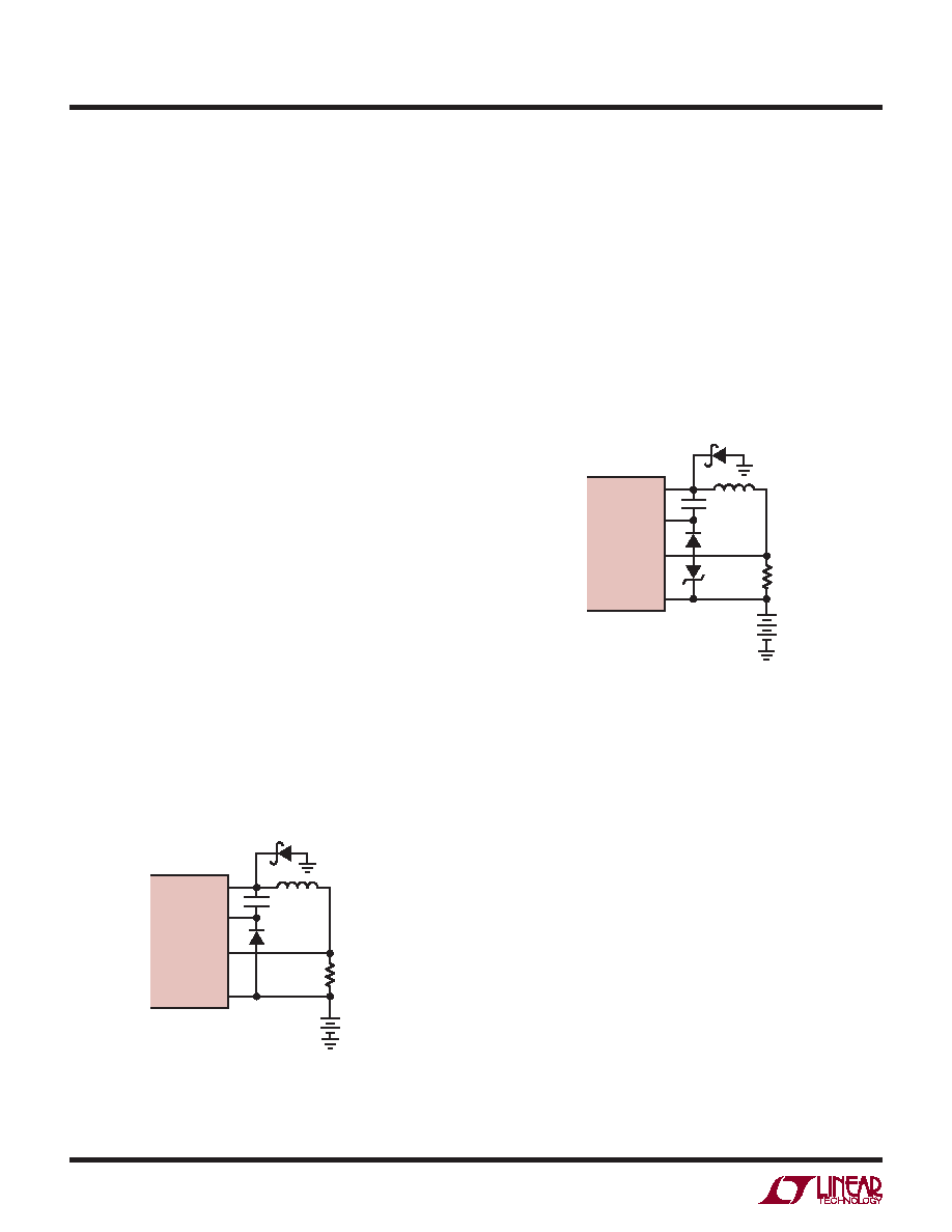
APPLICATIONS INFORMATION
Figure 1. Programming Maximum Charge
Current Using RSENSE
SW
BOOST
SENSE
BAT
RSENSE
LT3652HV
3652 F01
Figure 2. Zener Diode Reduces Refresh
Voltage for BOOST Pin
SW
BOOST
SENSE
BAT
LT3652HV
3652 F02
VIN / BOOST Start-Up Requirement
The LT3652HV operates with a VIN range of 4.95V to 34V,
however, a start-up voltage requirement exists due to
the nature of the non-synchronous step-down switcher
topology used for the charger. If there is no BOOST supply
available, the internal switch requires (VIN – VSW) ≥ 3.3V
to reliably operate. This requirement does not exist if the
BOOST supply is available and (VBOOST – VSW) > 2V.
When an LT3652HV charger is not switching, the SW pin
is at the same potential as the battery, which can be as
high as VBAT(FLT). As such, for reliable start-up, the VIN
supply must be at least 3.3V above VBAT(FLT). Once switch-
ing begins and the BOOST supply capacitor gets charged
such that (VBOOST – VSW) > 2V, the VIN requirement no
longer applies.
相关PDF资料 |
PDF描述 |
|---|---|
| LME0509SC | DC-DC REG PWR SUPPLY MODULE |
| LSN-1.5/10-D5B-C | DC-DC REG PWR SUPPLY MODULE |
| LSN-1.5/10-D5BH | DC-DC REG PWR SUPPLY MODULE |
| LSN-2.5/10-D5B-C | DC-DC REG PWR SUPPLY MODULE |
| LM2577MX-ADJ/NOPB | 6 A SWITCHING REGULATOR, 62 kHz SWITCHING FREQ-MAX, PDSO24 |
相关代理商/技术参数 |
参数描述 |
|---|---|
| LT3652HVIMSE-TRPBF | 制造商:LINER 制造商全称:Linear Technology 功能描述:Power Tracking 2A Battery Charger |
| LT3652IDD | 制造商:LINER 制造商全称:Linear Technology 功能描述:Power Tracking 2A Battery Charger for Solar Power |
| LT3652IDD#PBF | 功能描述:IC BATTERY CHARGER 2A 12DFN RoHS:是 类别:集成电路 (IC) >> PMIC - 电池管理 系列:- 产品培训模块:Lead (SnPb) Finish for COTS Obsolescence Mitigation Program 标准包装:2,500 系列:- 功能:电池监控器 电池化学:碱性,锂离子,镍镉,镍金属氢化物 电源电压:1 V ~ 5.5 V 工作温度:-40°C ~ 85°C 安装类型:表面贴装 封装/外壳:SOT-23-6 供应商设备封装:SOT-6 包装:带卷 (TR) |
| LT3652IDD#TRPBF | 功能描述:IC BATTERY CHARGER 2A 12DFN RoHS:是 类别:集成电路 (IC) >> PMIC - 电池管理 系列:- 产品培训模块:Lead (SnPb) Finish for COTS Obsolescence Mitigation Program 标准包装:2,500 系列:- 功能:电池监控器 电池化学:碱性,锂离子,镍镉,镍金属氢化物 电源电压:1 V ~ 5.5 V 工作温度:-40°C ~ 85°C 安装类型:表面贴装 封装/外壳:SOT-23-6 供应商设备封装:SOT-6 包装:带卷 (TR) |
| LT3652IDDPBF | 制造商:LINER 制造商全称:Linear Technology 功能描述:Power Tracking 2A Battery Charger for Solar Power |
发布紧急采购,3分钟左右您将得到回复。