- 您现在的位置:买卖IC网 > PDF目录44986 > LT3681EDE#TR (LINEAR TECHNOLOGY CORP) 4.4 A SWITCHING REGULATOR, 3100 kHz SWITCHING FREQ-MAX, PDSO14 PDF资料下载
参数资料
| 型号: | LT3681EDE#TR |
| 厂商: | LINEAR TECHNOLOGY CORP |
| 元件分类: | 稳压器 |
| 英文描述: | 4.4 A SWITCHING REGULATOR, 3100 kHz SWITCHING FREQ-MAX, PDSO14 |
| 封装: | 4 X 3 MM, PLASTIC, DFN-14 |
| 文件页数: | 10/24页 |
| 文件大小: | 367K |
| 代理商: | LT3681EDE#TR |
LT3681
18
3681f
Hot Plugging Safely
The small size, robustness and low impedance of ceramic
capacitors make them an attractive option for the input
bypass capacitor of LT3681 circuits. However, these
capacitors can cause problems if the LT3681 is plugged
into a live supply (see Linear Technology Application
Note 88 for a complete discussion). The low loss ceramic
capacitor, combined with stray inductance in series with
the power source, forms an under damped tank circuit,
and the voltage at the VIN pin of the LT3681 can ring
to twice the nominal input voltage, possibly exceeding
the LT3681’s rating and damaging the part. If the input
supply is poorly controlled or the user will be plugging
the LT3681 into an energized supply, the input network
should be designed to prevent this overshoot. Figure 10
shows the waveforms that result when an LT3681 circuit
is connected to a 24V supply through six feet of 24-gauge
twisted pair. The rst plot (10a) is the response with a
4.7F ceramic capacitor at the input. The input voltage
rings as high as 50V and the input current peaks at 26A.
A good solution is shown in Figure 10b. A 0.7
Ω resistor
is added in series with the input to eliminate the voltage
overshoot (it also reduces the peak inrush current). A
0.1F capacitor improves high frequency ltering. For
high input voltages its impact on efciency is minor,
reducing efciency by 1.5 percent for a 5V output at
full load operating from 24V. Another effective method
of reducing the overshoot is to add a 22F aluminum
electrolytic capacitor, as shown in Figure 10c.
High Temperature Considerations
The PCB must provide heat sinking to keep the LT3681
cool. The Exposed Pads on the bottom of the package
must be soldered to copper pours, which in turn should be
tied to large copper layers below with thermal vias; these
layers will spread the heat dissipated by the LT3681. Place
additional vias to reduce thermal resistance further. With
these steps, the thermal resistance from die (or junction)
to ambient can be reduced to
θJA = 35°C/W or less. With
100 LFPM airow, this resistance can fall by another 25%.
Further increases in airow will lead to lower thermal resis-
tance. Because of the large output current capability of the
LT3681, it is possible to dissipate enough power to raise
the junction temperature beyond the absolute maximum of
APPLICATIONS INFORMATION
125°C. When operating at high ambient temperatures, the
maximum load current should be derated as the ambient
temperature approaches 125°C.
Power dissipation within the LT3681 can be estimated
by calculating the total power loss from an efciency
measurement. The die temperature is calculated by
multiplying the LT3681 power dissipation by the thermal
resistance from junction to ambient.
Also keep in mind that the leakage current of the integrated
power Schottky diode, like all Schottky diodes, goes up
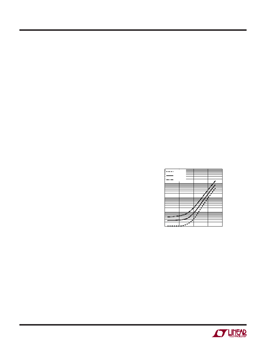
with junction temperature. The curves in Figure 11 show
how the leakage current in the power Schottky diode
varies with temperature and reverse voltage. When the
power switch is closed, the power Schottky diode is in
parallel with the power converter’s output lter stage. As
a result, an increase in a diode’s leakage current results
in an effective increase in the load, and a corresponding
increase in input power.
Figure 11. Like all Schottky Diodes, the LT3681 Integrated Power
Diode Leakage Current Varies with Temperature and Applied
Reverse Voltage VR.
TEMPERATURE (
°C)
–50
1
LEAKAGE
CURRENT
(
A)
100
10000
0
50
100
150
3681 F12
10
1000
VR = 10V
VR = 25V
VR = 40V
Other Linear Technology Publications
Application Notes 19, 35, 44 and 76 contain more detailed
descriptions and design information for buck regulators
and other switching regulators. The LT1376 data sheet
has a more extensive discussion of output ripple, loop
compensation and stability testing. Design Note 100
shows how to generate a bipolar output supply using a
buck regulator.
相关PDF资料 |
PDF描述 |
|---|---|
| LT3681EDE | 4.4 A SWITCHING REGULATOR, 3100 kHz SWITCHING FREQ-MAX, PDSO14 |
| LT3686AEMSE#PBF | 2.65 A SWITCHING REGULATOR, 2500 kHz SWITCHING FREQ-MAX, PDSO12 |
| LT3686AHMSE#TRPBF | 2.65 A SWITCHING REGULATOR, 2500 kHz SWITCHING FREQ-MAX, PDSO12 |
| LT3686AHMSE#PBF | 2.65 A SWITCHING REGULATOR, 2500 kHz SWITCHING FREQ-MAX, PDSO12 |
| LT3686AIMSE#TRPBF | 2.65 A SWITCHING REGULATOR, 2500 kHz SWITCHING FREQ-MAX, PDSO12 |
相关代理商/技术参数 |
参数描述 |
|---|---|
| LT3682 | 制造商:LINER 制造商全称:Linear Technology 功能描述:42V, 750mA Step-Down Regulator with 2.5μA |
| LT3682EDD#PBF | 功能描述:IC REG BUCK ADJ 1A 12DFN RoHS:是 类别:集成电路 (IC) >> PMIC - 稳压器 - DC DC 开关稳压器 系列:- 标准包装:250 系列:- 类型:降压(降压) 输出类型:固定 输出数:1 输出电压:1.2V 输入电压:2.05 V ~ 6 V PWM 型:电压模式 频率 - 开关:2MHz 电流 - 输出:500mA 同步整流器:是 工作温度:-40°C ~ 85°C 安装类型:表面贴装 封装/外壳:6-UFDFN 包装:带卷 (TR) 供应商设备封装:6-SON(1.45x1) 产品目录页面:1032 (CN2011-ZH PDF) 其它名称:296-25628-2 |
| LT3682EDD#TRPBF | 功能描述:IC REG BUCK ADJ 1A 12DFN RoHS:是 类别:集成电路 (IC) >> PMIC - 稳压器 - DC DC 开关稳压器 系列:- 标准包装:2,500 系列:- 类型:降压(降压) 输出类型:固定 输出数:1 输出电压:1.2V,1.5V,1.8V,2.5V 输入电压:2.7 V ~ 20 V PWM 型:- 频率 - 开关:- 电流 - 输出:50mA 同步整流器:是 工作温度:-40°C ~ 125°C 安装类型:表面贴装 封装/外壳:10-TFSOP,10-MSOP(0.118",3.00mm 宽)裸露焊盘 包装:带卷 (TR) 供应商设备封装:10-MSOP 裸露焊盘 |
| LT3682EDD-PBF | 制造商:LINER 制造商全称:Linear Technology 功能描述:1A Micropower Step-Down |
| LT3682EDD-TRPBF | 制造商:LINER 制造商全称:Linear Technology 功能描述:1A Micropower Step-Down |
发布紧急采购,3分钟左右您将得到回复。