- 您现在的位置:买卖IC网 > PDF目录44986 > LT3681EDE#TR (LINEAR TECHNOLOGY CORP) 4.4 A SWITCHING REGULATOR, 3100 kHz SWITCHING FREQ-MAX, PDSO14 PDF资料下载
参数资料
| 型号: | LT3681EDE#TR |
| 厂商: | LINEAR TECHNOLOGY CORP |
| 元件分类: | 稳压器 |
| 英文描述: | 4.4 A SWITCHING REGULATOR, 3100 kHz SWITCHING FREQ-MAX, PDSO14 |
| 封装: | 4 X 3 MM, PLASTIC, DFN-14 |
| 文件页数: | 7/24页 |
| 文件大小: | 367K |
| 代理商: | LT3681EDE#TR |
LT3681
15
3681f
Soft-Start
The RUN/SS pin can be used to soft-start the LT3681,
reducing the maximum input current during start-up.
The RUN/SS pin is driven through an external RC lter to
create a voltage ramp at this pin. Figure 7 shows the start-
up and shut-down waveforms with the soft-start circuit.
By choosing a large RC time constant, the peak start-up
current can be reduced to the current that is required to
regulate the output, with no overshoot. Choose the value
of the resistor so that it can supply 20A when the RUN/SS
pin reaches 2.3V.
Synchronization
The internal oscillator of the LT3681 can be synchronized
to an external 275kHz to 475kHz clock by using a 5pF
to 20pF capacitor to connect the clock signal to the RT
pin. The resistor tying the RT pin to ground should be
chosen such that the LT3681 oscillates 20% lower than
the intended synchronization frequency (see Setting the
Switching Frequency section).
The LT3681 should not be synchronized until its output
is near regulation as indicated by the PG ag. This can be
done with the system microcontroller/microprocessor or
with a discrete circuit by using the PG output. If a sync
signal is applied while the PG is low, the LT3681 may
exhibit erratic operation.
When applying a sync signal, positive clock transitions
reset LT3681’s internal clock and negative transitions
initiate a switch cycle. The amplitude of the sync signal
must be at least 2V. The sync signal duty cycle can range
from 5% up to a maximum value given by the following
equation:
DC
VV
V
f
SYNC MAX
OUT
D
IN
SW
D
SW
() =
+
16
–
– 0
00ns
where VOUT is the programmed output voltage, VD is the
diode forward drop, VIN is the typical input voltage, VSW
is the switch drop, and fSW is the desired switching fre-
quency. For example, a 24V input to 5V output at 300kHz
can be synchronized to a square wave with a maximum
duty cycle of 60%. For some applications, such as 12VIN
to 5VOUT at 350kHz, the maximum allowable sync duty
cycle will be less than 50%. If a low duty cycle clock cannot
be obtained from the system, then a one-shot should be
used between the sync signal and the LT3681. The value
of the coupling capacitor which connects the clock signal
to the RT pin should be chosen based on the clock signal
amplitude. Good starting values for 3.3V and 5V clock
signals are 10pF and 5pF, respectively. These values should
be tested and adjusted for each individual application to
assure reliable operation.
Figure 6. The Minimum Input Voltage Depends on
Output Voltage, Load Current and Boost Circuit
LOAD CURRENT (A)
0.001
INPUT
VOL
TAGE
(V)
4.0
4.5
5.0
10
3.5
3.0
2.0
0.01
0.1
1
2.5
6.0
5.5
3681 F06
LOAD CURRENT (A)
0.001
INPUT
VOL
TAGE
(V)
5.0
4.5
6.0
5.5
7.0
6.5
10
4.0
3.5
2.0
0.01
0.1
1
3.0
2.5
8.0
7.5
VOUT = 3.3V
TA = 25°C
L = 4.7
m
f = 800 kHz
TO START (RUN/SS = VIN)
TO START (RUN/SS CONTROL)
TO RUN
TO START (RUN/SS = VIN)
TO START (RUN/SS CONTROL)
TO RUN
VOUT = 5.0V
TA = 25°C
L = 4.7
m
f = 800 kHz
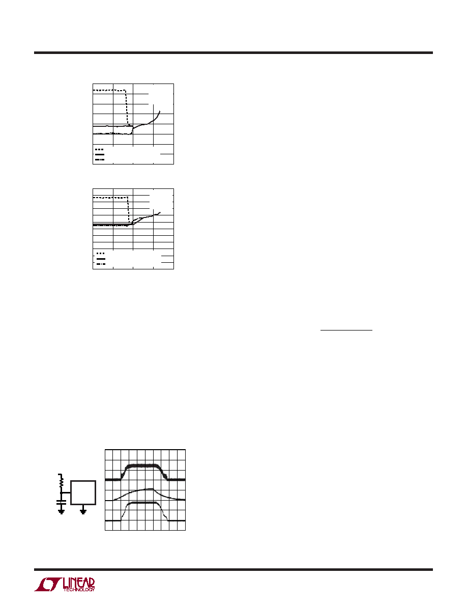
Figure 7. To Soft-Start the LT3681, Add a Resistor
and Capacitor to the RUN/SS Pin
3681 F07
IL
1A/DIV
VRUN/SS
2V/DIV
VOUT
2V/DIV
RUN/SS
GND
0.22
F
RUN
15k
2ms/DIV
APPLICATIONS INFORMATION
相关PDF资料 |
PDF描述 |
|---|---|
| LT3681EDE | 4.4 A SWITCHING REGULATOR, 3100 kHz SWITCHING FREQ-MAX, PDSO14 |
| LT3686AEMSE#PBF | 2.65 A SWITCHING REGULATOR, 2500 kHz SWITCHING FREQ-MAX, PDSO12 |
| LT3686AHMSE#TRPBF | 2.65 A SWITCHING REGULATOR, 2500 kHz SWITCHING FREQ-MAX, PDSO12 |
| LT3686AHMSE#PBF | 2.65 A SWITCHING REGULATOR, 2500 kHz SWITCHING FREQ-MAX, PDSO12 |
| LT3686AIMSE#TRPBF | 2.65 A SWITCHING REGULATOR, 2500 kHz SWITCHING FREQ-MAX, PDSO12 |
相关代理商/技术参数 |
参数描述 |
|---|---|
| LT3682 | 制造商:LINER 制造商全称:Linear Technology 功能描述:42V, 750mA Step-Down Regulator with 2.5μA |
| LT3682EDD#PBF | 功能描述:IC REG BUCK ADJ 1A 12DFN RoHS:是 类别:集成电路 (IC) >> PMIC - 稳压器 - DC DC 开关稳压器 系列:- 标准包装:250 系列:- 类型:降压(降压) 输出类型:固定 输出数:1 输出电压:1.2V 输入电压:2.05 V ~ 6 V PWM 型:电压模式 频率 - 开关:2MHz 电流 - 输出:500mA 同步整流器:是 工作温度:-40°C ~ 85°C 安装类型:表面贴装 封装/外壳:6-UFDFN 包装:带卷 (TR) 供应商设备封装:6-SON(1.45x1) 产品目录页面:1032 (CN2011-ZH PDF) 其它名称:296-25628-2 |
| LT3682EDD#TRPBF | 功能描述:IC REG BUCK ADJ 1A 12DFN RoHS:是 类别:集成电路 (IC) >> PMIC - 稳压器 - DC DC 开关稳压器 系列:- 标准包装:2,500 系列:- 类型:降压(降压) 输出类型:固定 输出数:1 输出电压:1.2V,1.5V,1.8V,2.5V 输入电压:2.7 V ~ 20 V PWM 型:- 频率 - 开关:- 电流 - 输出:50mA 同步整流器:是 工作温度:-40°C ~ 125°C 安装类型:表面贴装 封装/外壳:10-TFSOP,10-MSOP(0.118",3.00mm 宽)裸露焊盘 包装:带卷 (TR) 供应商设备封装:10-MSOP 裸露焊盘 |
| LT3682EDD-PBF | 制造商:LINER 制造商全称:Linear Technology 功能描述:1A Micropower Step-Down |
| LT3682EDD-TRPBF | 制造商:LINER 制造商全称:Linear Technology 功能描述:1A Micropower Step-Down |
发布紧急采购,3分钟左右您将得到回复。