参数资料
| 型号: | LT3681EDE#TRPBF |
| 厂商: | Linear Technology |
| 文件页数: | 14/24页 |
| 文件大小: | 0K |
| 描述: | IC REG BUCK ADJ 2A 14DFN |
| 标准包装: | 2,500 |
| 类型: | 降压(降压) |
| 输出类型: | 可调式 |
| 输出数: | 1 |
| 输出电压: | 1.27 V ~ 20 V |
| 输入电压: | 3.6 V ~ 34 V |
| PWM 型: | 电流模式,混合 |
| 频率 - 开关: | 300kHz ~ 2.8MHz |
| 电流 - 输出: | 2A |
| 同步整流器: | 无 |
| 工作温度: | -40°C ~ 85°C |
| 安装类型: | 表面贴装 |
| 封装/外壳: | 14-WFDFN 裸露焊盘 |
| 包装: | 带卷 (TR) |
| 供应商设备封装: | 14-DFN-EP(4x3) |
�� �
�
�LT3681�
�APPLICATIONS� INFORMATION�
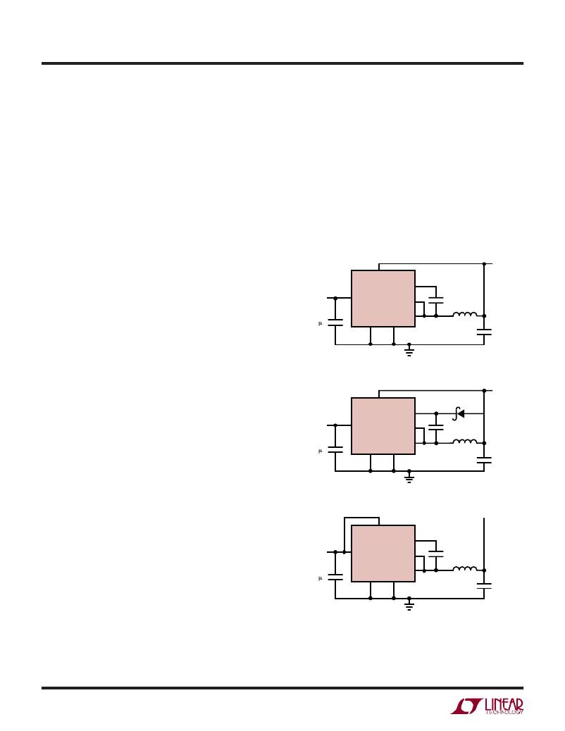
�BOOST� and� BIAS� Pin� Considerations�
�Capacitor� C3� and� the� internal� boost� Schottky� diode� (see�
�the� Block� Diagram)� are� used� to� generate� a� boost� volt-�
�age� that� is� higher� than� the� input� voltage.� In� most� cases�
�a� 0.22μF� capacitor� will� work� well.� Figure� 5� shows� three�
�ways� to� arrange� the� boost� circuit.� The� BOOST� pin� must� be�
�more� than� 2.3V� above� the� SW� pin� for� best� ef?ciency.� For�
�outputs� of� 2.8V� and� above,� the� standard� circuit� (Figure� 5a)�
�is� best.� For� outputs� between� 2.8V� and� 3V,� use� a� 1μF� boost�
�capacitor.� A� 2.5V� output� presents� a� special� case� because� it�
�is� marginally� adequate� to� support� the� boosted� drive� stage�
�while� using� the� internal� boost� diode.� For� reliable� BOOST� pin�
�operation� with� 2.5V� outputs� use� a� good� external� Schottky�
�boost� diode� can� be� tied� to� V� IN� ;� however,� this� restricts� the�
�input� range� to� one-half� of� the� absolute� maximum� rating�
�of� the� BOOST� pin.�
�At� light� loads,� the� inductor� current� becomes� discontinuous�
�and� the� effective� duty� cycle� at� the� BOOST� pin� (not� the� SW�
�pin)� can� be� very� high.� This� reduces� the� minimum� input�
�voltage� to� approximately� 300mV� above� V� OUT� .� At� higher� load�
�currents,� the� inductor� current� is� continuous� and� the� duty�
�cycle� is� limited� by� the� maximum� duty� cycle� of� the� LT3681,�
�requiring� a� higher� input� voltage� to� maintain� regulation.�
�V� OUT�
�diode� (such� as� the� ON� Semi� MBR0540),� and� a� 1μF� boost�
�capacitor� (see� Figure� 5b).� For� lower� output� voltages� the�
�boost� diode� can� be� tied� to� the� input� (Figure� 5c),� or� to�
�V� IN�
�V� IN�
�BD�
�LT3681�
�BOOST�
�DC�
�C3�
�another� supply� greater� than� 2.8V.� The� circuit� in� Figure� 5a�
�is� more� ef?cient� because� the� BOOST� pin� current� and� BIAS�
�4.7� F�
�GND�
�DA�
�SW�
�C� OUT�
�pin� quiescent� current� comes� from� a� lower� voltage� source.�
�You� must� also� be� sure� that� the� maximum� voltage� ratings�
�of� the� BOOST� and� BIAS� pins� are� not� exceeded.�
�The� minimum� operating� voltage� of� an� LT3681� application�
�(5a)� For� V� OUT� >� 2.8V�
�V� OUT�
�is� limited� by� the� minimum� input� voltage� (3.6V)� and� by� the�
�maximum� duty� cycle� as� outlined� in� a� previous� section.� For�
�BD�
�BOOST�
�D2�
�proper� startup,� the� minimum� input� voltage� is� also� limited�
�V� IN�
�V� IN�
�LT3681�
�DC�
�C3�
�by� the� boost� circuit.� If� the� input� voltage� is� ramped� slowly,�
�or� the� LT3681� is� turned� on� with� its� RUN/SS� pin� when� the�
�output� is� already� in� regulation,� then� the� boost� capacitor�
�4.7� F�
�GND�
�DA�
�SW�
�C� OUT�
�may� not� be� fully� charged.� Because� the� boost� capacitor� is�
�charged� with� the� energy� stored� in� the� inductor,� the� circuit�
�will� rely� on� some� minimum� load� current� to� get� the� boost�
�circuit� running� properly.� This� minimum� load� will� depend�
�on� input� and� output� voltages,� and� on� the� arrangement� of�
�(5b)� For� 2.5V� <� V� OUT� <� 2.8V�
�BD�
�V� OUT�
�the� boost� circuit.� The� minimum� load� generally� goes� to� zero�
�once� the� circuit� has� started.� If,� however,� the� LT3681� is�
�V� IN�
�V� IN�
�LT3681�
�BOOST�
�DC�
�C3�
�started� by� the� RUN/SS� pin� and� the� output� is� discharged,� the�
�discharged� output� capacitance� will� often� present� enough�
�of� a� load� to� allow� the� circuit� to� start.� Figure� 6� gives� plots�
�4.7� F�
�GND�
�DA�
�SW�
�C� OUT�
�of� the� input� voltage� required� for� three� different� situations:�
�the� worst� case� situation� where� RUN/SS� is� tied� to� V� IN� and�
�V� IN� is� ramped� up� very� slowly,� the� minimum� input� voltage�
�at� which� the� circuit� will� regulate� when� start-up� is� controlled�
�(5c)� For� V� OUT� <� 2.5V�
�3681� FO5�
�by� RUN/SS,� and� the� minimum� input� voltage� required� to�
�Figure� 5.� Three� Circuits� For� Generating� The� Boost� Voltage�
�maintain� output� regulation.� For� lower� start-up� voltage,� the�
�3681f�
�14�
�相关PDF资料 |
PDF描述 |
|---|---|
| LT3682IDD#TRPBF | IC REG BUCK ADJ 1A 12DFN |
| LT3684IMSE#TRPBF | IC REG BUCK ADJ 2A 10MSOP |
| LT3685IMSE#TRPBF | IC REG BUCK ADJ 2A 10MSOP |
| LT3686HDD#TRPBF | IC REG BUCK ADJ 1.2A 10DFN |
| LT3688HFE#TRPBF | IC REG BUCK ADJ 0.8A DL 24TSSOP |
相关代理商/技术参数 |
参数描述 |
|---|---|
| LT3682 | 制造商:LINER 制造商全称:Linear Technology 功能描述:42V, 750mA Step-Down Regulator with 2.5μA |
| LT3682EDD#PBF | 功能描述:IC REG BUCK ADJ 1A 12DFN RoHS:是 类别:集成电路 (IC) >> PMIC - 稳压器 - DC DC 开关稳压器 系列:- 标准包装:250 系列:- 类型:降压(降压) 输出类型:固定 输出数:1 输出电压:1.2V 输入电压:2.05 V ~ 6 V PWM 型:电压模式 频率 - 开关:2MHz 电流 - 输出:500mA 同步整流器:是 工作温度:-40°C ~ 85°C 安装类型:表面贴装 封装/外壳:6-UFDFN 包装:带卷 (TR) 供应商设备封装:6-SON(1.45x1) 产品目录页面:1032 (CN2011-ZH PDF) 其它名称:296-25628-2 |
| LT3682EDD#TRPBF | 功能描述:IC REG BUCK ADJ 1A 12DFN RoHS:是 类别:集成电路 (IC) >> PMIC - 稳压器 - DC DC 开关稳压器 系列:- 标准包装:2,500 系列:- 类型:降压(降压) 输出类型:固定 输出数:1 输出电压:1.2V,1.5V,1.8V,2.5V 输入电压:2.7 V ~ 20 V PWM 型:- 频率 - 开关:- 电流 - 输出:50mA 同步整流器:是 工作温度:-40°C ~ 125°C 安装类型:表面贴装 封装/外壳:10-TFSOP,10-MSOP(0.118",3.00mm 宽)裸露焊盘 包装:带卷 (TR) 供应商设备封装:10-MSOP 裸露焊盘 |
| LT3682EDD-PBF | 制造商:LINER 制造商全称:Linear Technology 功能描述:1A Micropower Step-Down |
| LT3682EDD-TRPBF | 制造商:LINER 制造商全称:Linear Technology 功能描述:1A Micropower Step-Down |
发布紧急采购,3分钟左右您将得到回复。