- 您现在的位置:买卖IC网 > PDF目录67758 > LT3682IDD#TRPBF (LINEAR TECHNOLOGY CORP) SWITCHING REGULATOR, PDSO12 PDF资料下载
参数资料
| 型号: | LT3682IDD#TRPBF |
| 厂商: | LINEAR TECHNOLOGY CORP |
| 元件分类: | 稳压器 |
| 英文描述: | SWITCHING REGULATOR, PDSO12 |
| 封装: | 3 X 3 MM, LEAD FREE, PLASTIC, DFN-12 |
| 文件页数: | 10/24页 |
| 文件大小: | 253K |
| 代理商: | LT3682IDD#TRPBF |
LT3682
18
3682f
APPLICATIONS INFORMATION
BOOST and BD Pin Considerations
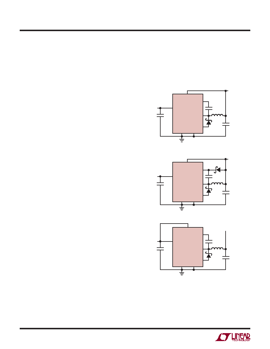
Capacitor C3 and the internal boost Schottky diode (see
the Block Diagram) are used to generate a boost volt-
age that is higher than the input voltage. In most cases
a 0.22μF capacitor will work well. Figure 5 shows three
ways to arrange the boost circuit. The BOOST pin must
be more than 2.3V above the SW pin for best efciency.
For outputs of between 3V and 8V, the standard circuit
(Figure 5a) is best. For outputs between 2.8V and 3V, use
a 1μF boost capacitor. A 2.5V output presents a special
case because it is marginally adequate to support the
boosted drive stage while using the internal boost diode.
For reliable BOOST pin operation with 2.5V outputs use
a good external Schottky diode (such as the ON Semi
MBR0540), and a 1μF boost capacitor (see Figure 5b).
For lower output voltages the boost diode can be tied to
the input (Figure 5c), or to another supply greater than
2.8V. Keep in mind that a minimum input voltage of 4.3V
is required if the voltage at the BD pin is smaller than 3V.
Tying BD to VIN reduces the maximum input voltage to
25V. The circuit in Figure 5a is more efcient because the
BOOST pin current and BD pin quiescent current come
from a lower voltage source. You must also be sure that
the maximum voltage ratings of the BOOST and BD pins
are not exceeded.
As mentioned, a minimum of 2.5V across the BOOST
capacitor is required for proper operation of the internal
BOOST circuitry to provide the base current for the power
NPN switch. For BD pin voltages higher than 3V, the excess
voltage across the BOOST capacitor does not bring an
increase in performance but dissipates additional power in
the internal BOOST circuitry instead. The BOOST circuitry
tolerates reasonable amounts of power, however excessive
power dissipation on this circuitry may impair reliability. For
reliable operation, use no more than 8V on the BD pin for
the circuit in Figure 5a. For higher output voltages, make
sure that there is no more than 8V at the BD pin either by
connecting it to another available supply higher than 3V or
by using a Zener diode between VOUT and BD to maintain
the BD pin voltage between 3V and 8V.
Figure 5. Three Circuits For Generating The Boost Voltage
(5a) For VOUT > 2.8V; VIN(MIN) = 4.3V if VOUT < 3V
LT3682
VIN
VOUT
VIN
BD
GND
SW
DA
BOOST
C3
D1
PGND
(5b) For 2.5V < VOUT < 2.8V; VIN(MIN) = 4.3V
(5c) For VOUT < 2.5V; VIN(MAX) = 25V
LT3682
VIN
VOUT
VIN
BD
GND
SW
DA
BOOST
C3
D1
D2
PGND
LT3682
VIN
VOUT
VIN
BD
GND
SW
DA
BOOST
C3
D1
PGND
3682 F05
The minimum operating voltage of an LT3682 applica-
tion is limited by the minimum input voltage and by the
maximum duty cycle as outlined previously. For proper
startup, the minimum input voltage is also limited by the
boost circuit. If the input voltage is ramped slowly, or the
LT3682 is turned on with its RUN/SS pin when the output
相关PDF资料 |
PDF描述 |
|---|---|
| LT3682EDD#TRPBF | SWITCHING REGULATOR, PDSO12 |
| LT3682EDD#PBF | SWITCHING REGULATOR, PDSO12 |
| LT5554IUH#TRPBF | SPECIALTY ANALOG CIRCUIT, PQCC32 |
| LT5554IUH#PBF | SPECIALTY ANALOG CIRCUIT, PQCC32 |
| LTC1421-2.5CSW#PBF | 1-CHANNEL POWER SUPPLY SUPPORT CKT, PDSO24 |
相关代理商/技术参数 |
参数描述 |
|---|---|
| LT3684 | 制造商:LINER 制造商全称:Linear Technology 功能描述:36V, 2A, 2.8MHz Step-Down Switching Regulator |
| LT3684EDD | 制造商:LINER 制造商全称:Linear Technology 功能描述:36V, 2A, 2.8MHz Step-Down Switching Regulator |
| LT3684EDD#PBF | 功能描述:IC REG BUCK ADJ 2A 10DFN RoHS:是 类别:集成电路 (IC) >> PMIC - 稳压器 - DC DC 开关稳压器 系列:- 标准包装:250 系列:- 类型:降压(降压) 输出类型:固定 输出数:1 输出电压:1.2V 输入电压:2.05 V ~ 6 V PWM 型:电压模式 频率 - 开关:2MHz 电流 - 输出:500mA 同步整流器:是 工作温度:-40°C ~ 85°C 安装类型:表面贴装 封装/外壳:6-UFDFN 包装:带卷 (TR) 供应商设备封装:6-SON(1.45x1) 产品目录页面:1032 (CN2011-ZH PDF) 其它名称:296-25628-2 |
| LT3684EDD#PBF | 制造商:Linear Technology 功能描述:DC-DC CONVERTER BUCK 2.8MHZ 制造商:Linear Technology 功能描述:DC-DC CONVERTER, BUCK, 2.8MHZ, DFN-10 |
| LT3684EDD#TRPBF | 功能描述:IC REG BUCK ADJ 2A 10DFN RoHS:是 类别:集成电路 (IC) >> PMIC - 稳压器 - DC DC 开关稳压器 系列:- 标准包装:2,500 系列:- 类型:降压(降压) 输出类型:固定 输出数:1 输出电压:1.2V,1.5V,1.8V,2.5V 输入电压:2.7 V ~ 20 V PWM 型:- 频率 - 开关:- 电流 - 输出:50mA 同步整流器:是 工作温度:-40°C ~ 125°C 安装类型:表面贴装 封装/外壳:10-TFSOP,10-MSOP(0.118",3.00mm 宽)裸露焊盘 包装:带卷 (TR) 供应商设备封装:10-MSOP 裸露焊盘 |
发布紧急采购,3分钟左右您将得到回复。