- 您现在的位置:买卖IC网 > PDF目录30768 > LT3695EMSE-3.3#TRPBF (LINEAR TECHNOLOGY CORP) 2 A SWITCHING REGULATOR, 2420 kHz SWITCHING FREQ-MAX, PDSO16 PDF资料下载
参数资料
| 型号: | LT3695EMSE-3.3#TRPBF |
| 厂商: | LINEAR TECHNOLOGY CORP |
| 元件分类: | 稳压器 |
| 英文描述: | 2 A SWITCHING REGULATOR, 2420 kHz SWITCHING FREQ-MAX, PDSO16 |
| 封装: | LEAD FREE, PLASTIC, MSOP-16 |
| 文件页数: | 10/30页 |
| 文件大小: | 491K |
| 代理商: | LT3695EMSE-3.3#TRPBF |
第1页第2页第3页第4页第5页第6页第7页第8页第9页当前第10页第11页第12页第13页第14页第15页第16页第17页第18页第19页第20页第21页第22页第23页第24页第25页第26页第27页第28页第29页第30页
LT3695 Series
18
3695fa
Low Ripple Burst Mode Operation
The LT3695 regulators are capable of operating in either
low ripple Burst Mode operation or pulse-skipping mode
which are selected using the SYNC pin. See the Synchro-
nization section for more information.
To enhance efciency at light loads, the LT3695 regulators
can be operated in low ripple Burst Mode operation which
keeps the output capacitor charged to the proper voltage
while minimizing the input quiescent current. During Burst
Mode operation, the LT3695 regulators deliver single
cycle bursts of current to the output capacitor followed by
sleep periods where the output power is delivered to the
load by the output capacitor. Because the LT3695 regula-
tors deliver power to the output with single, low current
pulses, the output ripple is kept below 15mV for a typical
application. In addition, VIN and BD (LT3695), and OUT1,2
(LT3695-3.3, LT3695-5) quiescent currents are reduced
to typically 35μA, 55μA and 65μA, respectively, during
the sleep time. As the load current decreases towards a
no-load condition, the percentage of time that the LT3695
regulators operate in sleep mode increases and the average
input current is greatly reduced resulting in high efciency
even at very low loads (see Figure 3). At higher output
loads (above about 70mA for the front page application)
the LT3695 regulators will be running at the frequency
programmed by the RT resistor, and will be operating in
standard PWM mode. The transition between PWM and
low ripple Burst Mode operation is seamless, and will not
disturb the output voltage.
If low quiescent current is not required, tie SYNC high to
select pulse-skipping mode. The benet of this mode is
that the LT3695 regulators will enter full frequency standard
PWM operation at a lower output load current than when
in Burst Mode operation. With the SYNC pin tied low, the
front page application circuit will switch at full frequency
at output loads higher than about 100mA. With the SYNC
pin tied high, the front page application circuit will switch
at full frequency at output loads higher than about 30mA.
The maximum load current that the LT3695 regulators can
supply is reduced when SYNC is high.
BOOST Pin Considerations
Capacitor C3 and the internal boost Schottky diode (see the
Block Diagram) are used to generate a boost voltage that
is higher than the input voltage. In most cases a 0.22μF
capacitor will work well. Figure 4 shows three ways to
arrange the boost circuit for the LT3695 regulators. The
BOOST pin must be more than 2.3V above the SW pin
for best efciency. For outputs of between 3V and 8V, the
standard circuit (Figure 4a) is best. For outputs between
2.8V and 3V, use a 1μF boost capacitor. A 2.5V output
presents a special case because it is marginally adequate
to support the boosted drive stage while using the internal
boost diode. For reliable BOOST pin operation with 2.5V
outputs use a good external Schottky diode (such as the
ON Semi MBR0540), and a 1μF boost capacitor (see Figure
4b). For lower output voltages the boost diode can be tied
to the input (Figure 4c), or to another supply greater than
2.8V. Keep in mind that a minimum input voltage of 4.3V
is required if the voltage at the BD pin is smaller than 3V.
Tying BD to VIN reduces the maximum input voltage to
25V. The circuit in Figure 4a is more efcient because the
BOOST pin current and BD pin quiescent current come
from a lower voltage source. You must also be sure that
the maximum voltage ratings of the BOOST and BD pins
are not exceeded.
As mentioned, a minimum of 2.5V across the BOOST
capacitor is required for proper operation of the internal
BOOST circuitry to provide the base current for the power
NPN switch. For BD pin voltages higher than 3V, the excess
voltage across the BOOST capacitor does not bring an
increase in performance but dissipates additional power in
the internal BOOST circuitry instead. The BOOST circuitry
tolerates reasonable amounts of power, however excessive
power dissipation on this circuitry may impair reliability. For
reliable operation, use no more than 8V on the BD pin for
APPLICATIONS INFORMATION
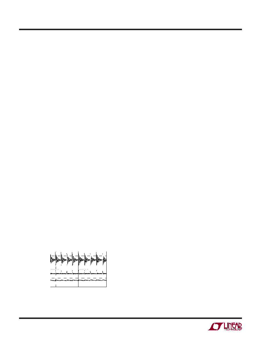
Figure 3. Switching Waveforms, Burst Mode Operation
5μs/DIV
VSW
5V/DIV
VOUT
20mV/DIV
IL
0.2A/DIV
VIN = 12V, FRONT PAGE APPLICATION
ILOAD = 5mA
3695 F03
相关PDF资料 |
PDF描述 |
|---|---|
| LT3751IUFD#TR | 1-CHANNEL POWER SUPPLY SUPPORT CKT, PQCC20 |
| LT3751IUFD#TRPBF | 1-CHANNEL POWER SUPPLY SUPPORT CKT, PQCC20 |
| LT3751EFE | 1-CHANNEL POWER SUPPLY SUPPORT CKT, PDSO20 |
| LT3751EUFD#TRPBF | 1-CHANNEL POWER SUPPLY SUPPORT CKT, PQCC20 |
| LT3751EUFD | 1-CHANNEL POWER SUPPLY SUPPORT CKT, PQCC20 |
相关代理商/技术参数 |
参数描述 |
|---|---|
| LT3695EMSE-5#PBF | 功能描述:IC REG BUCK 5V 1A 16MSOP RoHS:是 类别:集成电路 (IC) >> PMIC - 稳压器 - DC DC 开关稳压器 系列:- 标准包装:250 系列:- 类型:降压(降压) 输出类型:固定 输出数:1 输出电压:1.2V 输入电压:2.05 V ~ 6 V PWM 型:电压模式 频率 - 开关:2MHz 电流 - 输出:500mA 同步整流器:是 工作温度:-40°C ~ 85°C 安装类型:表面贴装 封装/外壳:6-UFDFN 包装:带卷 (TR) 供应商设备封装:6-SON(1.45x1) 产品目录页面:1032 (CN2011-ZH PDF) 其它名称:296-25628-2 |
| LT3695EMSE-5#PBF | 制造商:Linear Technology 功能描述:IC STEP-DOWN REGULATOR MSOP-16 |
| LT3695EMSE-5#TRPBF | 功能描述:IC REG BUCK 5V 1A 16MSOP RoHS:是 类别:集成电路 (IC) >> PMIC - 稳压器 - DC DC 开关稳压器 系列:- 标准包装:2,500 系列:- 类型:降压(降压) 输出类型:固定 输出数:1 输出电压:1.2V,1.5V,1.8V,2.5V 输入电压:2.7 V ~ 20 V PWM 型:- 频率 - 开关:- 电流 - 输出:50mA 同步整流器:是 工作温度:-40°C ~ 125°C 安装类型:表面贴装 封装/外壳:10-TFSOP,10-MSOP(0.118",3.00mm 宽)裸露焊盘 包装:带卷 (TR) 供应商设备封装:10-MSOP 裸露焊盘 |
| LT3695EMSEPBF | 制造商:LINER 制造商全称:Linear Technology 功能描述:1A Fault Tolerant Micropower Step-Down Regulator |
| LT3695EMSETRPBF | 制造商:LINER 制造商全称:Linear Technology 功能描述:1A Fault Tolerant Micropower Step-Down Regulator |
发布紧急采购,3分钟左右您将得到回复。