- 您现在的位置:买卖IC网 > PDF目录30768 > LT3695EMSE-3.3#TRPBF (LINEAR TECHNOLOGY CORP) 2 A SWITCHING REGULATOR, 2420 kHz SWITCHING FREQ-MAX, PDSO16 PDF资料下载
参数资料
| 型号: | LT3695EMSE-3.3#TRPBF |
| 厂商: | LINEAR TECHNOLOGY CORP |
| 元件分类: | 稳压器 |
| 英文描述: | 2 A SWITCHING REGULATOR, 2420 kHz SWITCHING FREQ-MAX, PDSO16 |
| 封装: | LEAD FREE, PLASTIC, MSOP-16 |
| 文件页数: | 17/30页 |
| 文件大小: | 491K |
| 代理商: | LT3695EMSE-3.3#TRPBF |
第1页第2页第3页第4页第5页第6页第7页第8页第9页第10页第11页第12页第13页第14页第15页第16页当前第17页第18页第19页第20页第21页第22页第23页第24页第25页第26页第27页第28页第29页第30页
LT3695 Series
24
3695fa
+ R2, and the BD pin (if connected to VOUT) in the case of
the LT3695, or by RLOAD, R4 and the OUT1,2 pins in the
case of the LT3695-3.3 and LT3695-5. Since this causes
VOUT to rise, the LT3695 regulators stop switching. The
resistive divider formed by R3, RLOAD and R1 + R2 and
R4, respectively, must be adjusted for VOUT not to exceed
its nominal value at the required maximum input voltage
VIN(MAX). R3 must supply sufcient current into RUN/SS
at the required minimum input voltage VIN(MIN) for normal
non-fault situations. Based on the maximum RUN/SS cur-
rent of 7.5μA at VRUN/SS = 2.5V this gives
R
VV
A
IN MIN
3
25
75
≤
() –.
.
The current through R3 is maximal at VIN(MAX)withRUN/SS
shorted to SW:
I
VV
R
IN MAX
OUT
3
=
() –
For the LT3695, this current must be drawn by RLOAD,
R1 + R2, and the BD pin, if connected to VOUT:
I
V
RR
R
I
R
OUT
LOAD
BD
3
12
≤
+
()
+
||
Without load (RLOAD = ∞) and assuming the minimum
current of 35μA into the BD pin, this leads to
RR
V
VV
R
A
OUT
IN MAX
OUT
12
3
35
+
≤
() –
–
as upper limit for the feedback resistors. For VOUT < 2.5V
assume no current drawn by the BD pin, which gives
RR
VR
VV
OUT
IN MAX
OUT
12
3
+
≤
–
()
For the LT3695-3.3 and LT3695-5, the current through R3
must be drawn by RLOAD, R4 and the OUT1,2 pins:
I
V
RR
I
R
OUT
LOAD
OUT
312
4
≤
+
||
,
Without load (RLOAD = ∞) and assuming the minimum
current of 43μA into the OUT1,2 pins, this leads to:
R
V
VV
R
A
OUT
IN MAX
OUT
4
3
43
≤
() –
–
as upper limit for R4. Depending on the required input
voltage range, R4 may be omitted.
Tables 7 and 8 show example values for common appli-
cations. RSS must be included as the switch node would
otherwise have to charge CSS if the SW pin and the RUN/SS
pin are shorted, which may damage the power switch.
If RUN/SS is controlled by an external circuitry, the current
this circuitry can supply must be limited. This can be done
as discussed above. In addition, it may be necessary to
protect this external circuitry from the voltage at SW, for
example by using a diode.
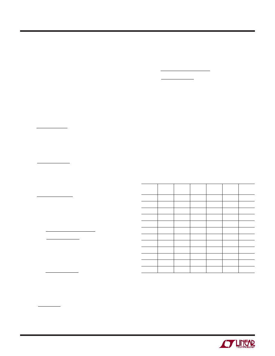
Table 7. LT3695: Example Values for R1, R2 and R3 for Common
Combinations of VIN and VOUT. IR1+R2 is the Current Drawn by
R1 + R2 in Normal Operation
VIN(MAX)
(V)
VIN(MIN)
(V)
VOUT
(V)
R3
(kΩ)
R1
(kΩ)
R2
(kΩ)
IR1+R2
(μA)
16
3.8
1.8
169
11.5
9.09
87
36
3.8
1.8
169
4.75
3.74
212
16
4.5
2.5
261
93.1
43.2
18
36
4.5
2.5
261
16.9
7.87
101
16
5.3
3.3
365
432
137
6
36
5.3
3.3
365
43.2
13.7
58
16
7
5
274
536
102
8
36
7
5
590
221
42.2
19
16
10
8
200
562
61.9
13
36
10
8
475
280
30.9
26
27
14
12
301
511
36.5
22
36
14
12
442
511
36.5
22
APPLICATIONS INFORMATION
相关PDF资料 |
PDF描述 |
|---|---|
| LT3751IUFD#TR | 1-CHANNEL POWER SUPPLY SUPPORT CKT, PQCC20 |
| LT3751IUFD#TRPBF | 1-CHANNEL POWER SUPPLY SUPPORT CKT, PQCC20 |
| LT3751EFE | 1-CHANNEL POWER SUPPLY SUPPORT CKT, PDSO20 |
| LT3751EUFD#TRPBF | 1-CHANNEL POWER SUPPLY SUPPORT CKT, PQCC20 |
| LT3751EUFD | 1-CHANNEL POWER SUPPLY SUPPORT CKT, PQCC20 |
相关代理商/技术参数 |
参数描述 |
|---|---|
| LT3695EMSE-5#PBF | 功能描述:IC REG BUCK 5V 1A 16MSOP RoHS:是 类别:集成电路 (IC) >> PMIC - 稳压器 - DC DC 开关稳压器 系列:- 标准包装:250 系列:- 类型:降压(降压) 输出类型:固定 输出数:1 输出电压:1.2V 输入电压:2.05 V ~ 6 V PWM 型:电压模式 频率 - 开关:2MHz 电流 - 输出:500mA 同步整流器:是 工作温度:-40°C ~ 85°C 安装类型:表面贴装 封装/外壳:6-UFDFN 包装:带卷 (TR) 供应商设备封装:6-SON(1.45x1) 产品目录页面:1032 (CN2011-ZH PDF) 其它名称:296-25628-2 |
| LT3695EMSE-5#PBF | 制造商:Linear Technology 功能描述:IC STEP-DOWN REGULATOR MSOP-16 |
| LT3695EMSE-5#TRPBF | 功能描述:IC REG BUCK 5V 1A 16MSOP RoHS:是 类别:集成电路 (IC) >> PMIC - 稳压器 - DC DC 开关稳压器 系列:- 标准包装:2,500 系列:- 类型:降压(降压) 输出类型:固定 输出数:1 输出电压:1.2V,1.5V,1.8V,2.5V 输入电压:2.7 V ~ 20 V PWM 型:- 频率 - 开关:- 电流 - 输出:50mA 同步整流器:是 工作温度:-40°C ~ 125°C 安装类型:表面贴装 封装/外壳:10-TFSOP,10-MSOP(0.118",3.00mm 宽)裸露焊盘 包装:带卷 (TR) 供应商设备封装:10-MSOP 裸露焊盘 |
| LT3695EMSEPBF | 制造商:LINER 制造商全称:Linear Technology 功能描述:1A Fault Tolerant Micropower Step-Down Regulator |
| LT3695EMSETRPBF | 制造商:LINER 制造商全称:Linear Technology 功能描述:1A Fault Tolerant Micropower Step-Down Regulator |
发布紧急采购,3分钟左右您将得到回复。