- 您现在的位置:买卖IC网 > PDF目录15239 > LT3724MPFE#PBF (Linear Technology)IC REG CTRLR BST INV PWM 16TSSOP PDF资料下载
参数资料
| 型号: | LT3724MPFE#PBF |
| 厂商: | Linear Technology |
| 文件页数: | 9/26页 |
| 文件大小: | 0K |
| 描述: | IC REG CTRLR BST INV PWM 16TSSOP |
| 标准包装: | 95 |
| PWM 型: | 电流模式 |
| 输出数: | 1 |
| 频率 - 最大: | 225kHz |
| 占空比: | 100% |
| 电源电压: | 4 V ~ 60 V |
| 降压: | 是 |
| 升压: | 是 |
| 回扫: | 无 |
| 反相: | 是 |
| 倍增器: | 无 |
| 除法器: | 无 |
| Cuk: | 无 |
| 隔离: | 无 |
| 工作温度: | -55°C ~ 125°C |
| 封装/外壳: | 16-TSSOP(0.173",4.40mm)裸露焊盘 |
| 包装: | 管件 |
�� �
�
�LT3724�
�OPERATIONS�
�(Refer� to� Functional� Diagram)�
�The� LT3724� is� a� PWM� controller� with� a� constant� frequency,�
�current� mode� control� architecture.� It� is� designed� for� low�
�to� medium� power,� switching� regulator� applications.� Its�
�high� operating� voltage� capability� allows� it� to� step-up�
�or� down� input� voltages� up� to� 60V� without� the� need� for�
�a� transformer.� The� LT3724� is� used� in� nonsynchronous�
�applications,� meaning� that� a� freewheeling� rectifier� diode�
�(D1� of� Function� Diagram)� is� used� instead� of� a� bottom�
�side� MOSFET.� For� circuit� operation,� please� refer� to� the�
�Functional� Diagram� of� the� IC� and� Typical� Application� on�
�the� front� page� of� the� data� sheet.� The� LT3800� is� a� similar�
�part� that� uses� synchronous� rectification,� replacing� the�
�diode� with� a� MOSFET� in� a� step-down� application.�
�Main� Control� Loop�
�During� normal� operation,� the� external� N-channel� MOSFET�
�switch� is� turned� on� at� the� beginning� of� each� cycle.� The�
�switch� stays� on� until� the� current� in� the� inductor� exceeds�
�a� current� threshold� set� by� the� DC� control� voltage,� V� C� ,� the�
�output� of� the� voltage� control� loop.� The� voltage� control� loop�
�monitors� the� output� voltage,� via� the� V� FB� pin� voltage,� and�
�compares� it� to� an� internal� 1.231V� reference.� It� increases�
�the� current� threshold� when� the� V� FB� voltage� is� below� the�
�reference� voltage� and� decreases� the� current� threshold�
�when� the� V� FB� voltage� is� above� the� reference� voltage.� For�
�instance,� when� an� increase� in� the� load� current� occurs,�
�the� output� voltage� drops� causing� the� V� FB� voltage� to� drop�
�relative� to� the� 1.231V� reference.� The� voltage� control� loop�
�senses� the� drop� and� increases� the� current� threshold.� The�
�peak� inductor� current� is� increased� until� the� average� induc-�
�tor� current� equals� the� new� load� current� and� the� output�
�voltage� returns� to� regulation.�
�Current� Limit/Short-Circuit�
�The� inductor� current� is� measured� with� a� series� sense�
�resistor� (see� the� Typical� Application� on� the� front� page).�
�When� the� voltage� across� the� sense� resistor� reaches� the�
�maximum� current� sense� threshold,� typically� 150mV,� the�
�TG� MOSFET� driver� is� disabled� for� the� remainder� of� that�
�cycle.� If� the� maximum� current� sense� threshold� is� still� ex-�
�ceeded� at� the� beginning� of� the� next� cycle,� the� entire� cycle�
�is� skipped.� Cycle� skipping� keeps� the� inductor� currents� to�
�a� controlled� value� during� a� short-circuit,� particularly� when�
�V� IN� is� high.� Setting� the� sense� resistor� value� is� discussed�
�in� the� “Application� Information”� section.�
�V� CC� /Boosted� Supply�
�An� internal� V� CC� regulator� provides� V� IN� derived� gate-drive�
�power� for� start-up� under� all� operating� conditions� with�
�MOSFET� gate� charge� loads� up� to� 90nC.� The� regulator� can�
�operate� continuously� in� applications� with� V� IN� voltages�
�up� to� 60V,� provided� the� V� IN� voltage� and/or� MOSFET� gate�
�charge� currents� do� not� create� excessive� power� dissipa-�
�tion� in� the� IC.� Safe� operating� conditions� for� continuous�
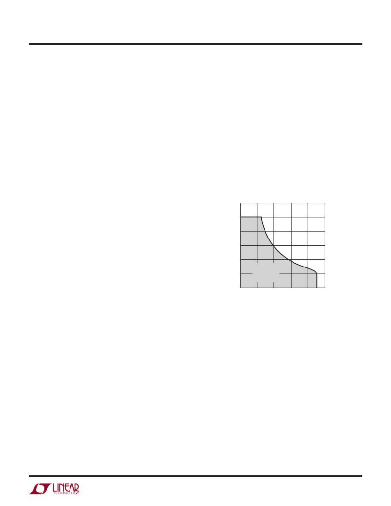
�regulator� use� are� shown� in� Figure� 1.� In� applications� where�
�these� conditions� are� exceeded,� V� CC� must� be� derived� from�
�an� external� source� after� start-up.� The� LT3724� regulator�
�can,� however,� be� used� for� “full� time”� use� in� applications�
�where� short-duration� V� IN� transients� exceed� allowable�
�continuous� voltages.�
�70�
�60�
�50�
�40�
�30�
�SAFE�
�20� OPERATING�
�AREA�
�10�
�0� 20� 40� 60� 80� 100�
�MOSFET� TOTAL� GATE� CHARGE� (nC)�
�3724� F01�
�Figure� 1.� V� CC� Regulator� Continuous� Operating� Conditions�
�For� higher� converter� efficiency� and� less� power� dissipa-�
�tion� in� the� IC,� V� CC� can� also� be� supplied� from� an� external�
�supply� such� as� the� converter� output.� When� an� external�
�supply� back� drives� the� internal� V� CC� regulator� through� an�
�external� diode� and� the� V� CC� voltage� is� pulled� to� a� diode�
�above� its� regulation� voltage,� the� internal� regulator� is� dis-�
�abled� and� goes� into� a� low� current� mode.� V� CC� is� the� bias�
�supply� for� most� of� the� internal� IC� functions� and� is� also�
�used� to� charge� the� bootstrapped� capacitor� (C� BOOST� )� via� an�
�external� diode.� The� external� MOSFET� switch� is� biased� from�
�the� bootstrapped� capacitor.� While� the� external� MOSFET�
�switch� is� off,� an� internal� BJT� switch,� whose� collector� is�
�connected� to� the� SW� pin� and� emitter� is� connected� to� the�
�PGND� pin,� is� turned� on� to� pull� the� SW� node� to� PGND� and�
�recharge� the� bootstrap� capacitor.� The� switch� stays� on� until�
�3724fd�
�9�
�相关PDF资料 |
PDF描述 |
|---|---|
| LTC3729EUH | IC REG CTRLR BUCK PWM CM 32-QFN |
| VI-25Z-EU-F1 | CONVERTER MOD DC/DC 2V 80W |
| SRP1040-R75M | INDUCTOR 750NH 22A SMD |
| LTC3880IUJ#TRPBF | IC REG CTRLR BUCK PWM CM 40-QFN |
| SRP1040-R56M | INDUCTOR 560NH 25A SMD |
相关代理商/技术参数 |
参数描述 |
|---|---|
| LT3724MPFE-TR | 制造商:LINER 制造商全称:Linear Technology 功能描述:High Voltage, Current Mode Switching Regulator Controller |
| LT3726EGN | 制造商:Linear Technology 功能描述: |
| LT373L | 制造商:未知厂家 制造商全称:未知厂家 功能描述:Optoelectronic |
| LT373LF | 制造商:EDSYN 功能描述:LONER Angle Face Soldring Tip High-Temperature Rated for Lead-Free Process W: .0 |
发布紧急采购,3分钟左右您将得到回复。