- 您现在的位置:买卖IC网 > PDF目录1825 > LT3740EDHC#PBF (Linear Technology)IC REG CTRLR BUCK PWM CM 16-DFN PDF资料下载
参数资料
| 型号: | LT3740EDHC#PBF |
| 厂商: | Linear Technology |
| 文件页数: | 5/20页 |
| 文件大小: | 0K |
| 描述: | IC REG CTRLR BUCK PWM CM 16-DFN |
| 标准包装: | 73 |
| PWM 型: | 电流模式 |
| 输出数: | 1 |
| 频率 - 最大: | 330kHz |
| 占空比: | 90% |
| 电源电压: | 2.2 V ~ 22 V |
| 降压: | 是 |
| 升压: | 无 |
| 回扫: | 无 |
| 反相: | 无 |
| 倍增器: | 无 |
| 除法器: | 无 |
| Cuk: | 无 |
| 隔离: | 无 |
| 工作温度: | -40°C ~ 85°C |
| 封装/外壳: | 16-WFDFN 裸露焊盘 |
| 包装: | 管件 |
| 产品目录页面: | 1332 (CN2011-ZH PDF) |
�� �
�
�LT3740�
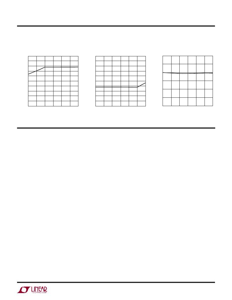
�TYPICAL� PERFORMANCE� CHARACTERISTICS�
�(T� A� =� 25°C,� unless� otherwise� noted)�
�400�
�390�
�380�
�370�
�360�
�350�
�340�
�330�
�320�
�310�
�Error� Ampli?er� Transconductance�
�vs� Temperature�
�7.50�
�7.45�
�7.40�
�7.35�
�7.30�
�7.25�
�7.20�
�7.15�
�7.10�
�7.05�
�BIAS-V� IN� to� Enable� Controller�
�vs� Temperature�
�3.0�
�2.5�
�2.0�
�1.5�
�1.0�
�0.5�
�Undervoltage� Lockout� Threshold�
�vs� Temperature�
�300�
�–50�
�–25�
�0�
�25� 50�
�75�
�100�
�7.00�
�–50�
�–25�
�0�
�25� 50�
�75�
�100�
�0�
�–50�
�–25�
�0�
�25� 50�
�75�
�100�
�TEMPERATURE� (°C)�
�PIN� FUNCTIONS�
�3740� G12�
�TEMPERATURE� (°C)�
�3740� G13�
�TEMPERATURE� (°C)�
�3740� G14�
�SN� –� (Pin� 1):� Negative� Current� Sensing� Pin.� Connect� this�
�pin� to� the� source� of� the� bottom� MOSFET� for� No� R� SENSE�
�or� to� a� current� sense� resistor.�
�PGND� (Pin� 2):� Power� Ground.� Connect� this� pin� closely� to�
�the� source� of� the� bottom� N-channel� MOSFET.�
�BGATE� (Pin� 3):� Bottom� Gate� Drive.� Drives� the� gate� of� the�
�bottom� N-channel� MOSFET.�
�BGDP� (Pin� 4):� Bottom� Gate� Drive� Power� Supply.� Connect�
�this� pin� to� a� voltage� source� higher� than� 7V� (V� IN� or� BIAS).�
�SN� +� (Pin� 5):� Positive� Current� Sensing� Pin.� Connect� this�
�pin� to� the� drain� of� the� bottom� MOSFET� for� No� R� SENSE� or�
�to� a� current� sense� resistor.�
�SW� (Pin� 6):� Switch� Node.� Connect� this� pin� to� the� source�
�of� the� top� N-channel� MOSFET� and� the� drain� of� the� bottom�
�N-channel� MOSFET.�
�TGATE� (Pin� 7):� Top� Gate� Drive.� Drives� the� gate� of� the� top�
�N-channel� MOSFET� to� BIAS.�
�BIAS� (Pin� 8):� Top� Gate� Drive� Power� Supply.� Connect� a�
�capacitor� between� this� pin� and� V� IN� .�
�SWB� (Pin� 9):� Switch� Pin� of� the� Internal� Boost.� Connect�
�V� IN� (Pin� 10):� Input� Supply� Pin.� Must� be� locally� bypassed�
�with� a� capacitor.�
�RANGE� (Pin� 11):� Current� Limit� Range� Select� Pin.� Ground�
�this� pin� for� 50mV� current� sense� voltage� limit.� Leave� this�
�pin� open� for� 80mV� current� sense� voltage� limit.� Connect�
�this� pin� to� V� IN� for� current� sense� voltage� limit� of� 105mV.�
�PGOOD� (Pin� 12):� Power� Good� Output.� Open� collector�
�logic� output� that� is� pulled� low� when� the� FB� voltage� lower�
�than� 720mV.�
�SHDN� (Pin� 13):� Shutdown� Pin.� Connect� to� 2.5V� or� higher� to�
�enable� device;� 0.5V� or� less� to� disable� device.� Also,� this� pin�
�functions� as� soft-start� when� a� voltage� ramp� is� applied.�
�XREF� (Pin� 14):� External� Reference� Pin.� This� pin� sets� the�
�FB� voltage� externally� between� 0V� and� 0.8V.� It� can� be� used�
�to� slave� the� output� voltage� during� normal� operation� or� the�
�output� start-up� behavior� to� an� external� signal� source.� Tie�
�this� pin� to� 1V� or� higher� to� use� the� internal� 0.8V� reference.�
�FB� (Pin� 15):� Feedback� Pin.� Pin� voltage� is� regulated� to� 0.8V�
�if� internal� reference� is� used� or� to� the� XREF� pin� if� voltage�
�is� between� 0V� and� 0.8V.� Connect� the� feedback� resistor�
�divider� to� this� pin.�
�the� boost� inductor� here.�
�3740fc�
�5�
�相关PDF资料 |
PDF描述 |
|---|---|
| LT3741EFE#PBF | IC REG CTRLR BUCK PWM CM 20TSSOP |
| LT3742EUF#PBF | IC REG CTRLR BUCK PWM CM 24-QFN |
| LT3748HMS#PBF | IC REG CTRLR FLYBK ISO CM 16MSOP |
| LT3757EDD#PBF | IC REG CTRLR BST FLYBK INV 10DFN |
| LT3758EMSE#PBF | IC REG CTRLR PWM CM 10-MSOP |
相关代理商/技术参数 |
参数描述 |
|---|---|
| LT3740EDHC-TR | 制造商:LINER 制造商全称:Linear Technology 功能描述:Wide Operating Range, Valley Mode, No RSENSE? Synchronous Step-Down Controller |
| LT3740EDHC-TRPBF | 制造商:LINER 制造商全称:Linear Technology 功能描述:Wide Operating Range, Valley Mode, No RSENSE? Synchronous Step-Down Controller |
| LT3741 | 制造商:LINER 制造商全称:Linear Technology 功能描述:High Voltage, Current Mode Switching Regulator Controller Thermal Shutdown |
| LT3741EFE#PBF | 功能描述:IC REG CTRLR BUCK PWM CM 20TSSOP RoHS:是 类别:集成电路 (IC) >> PMIC - 稳压器 - DC DC 切换控制器 系列:- 特色产品:LM3753/54 Scalable 2-Phase Synchronous Buck Controllers 标准包装:1 系列:PowerWise® PWM 型:电压模式 输出数:1 频率 - 最大:1MHz 占空比:81% 电源电压:4.5 V ~ 18 V 降压:是 升压:无 回扫:无 反相:无 倍增器:无 除法器:无 Cuk:无 隔离:无 工作温度:-5°C ~ 125°C 封装/外壳:32-WFQFN 裸露焊盘 包装:Digi-Reel® 产品目录页面:1303 (CN2011-ZH PDF) 其它名称:LM3754SQDKR |
| LT3741EFE#PBF | 制造商:Linear Technology 功能描述:DC-DC CONTROLLER BUCK 1MHZ 制造商:Linear Technology 功能描述:DC-DC CONTROLLER, BUCK, 1MHZ, TSSOP-20 |
发布紧急采购,3分钟左右您将得到回复。