- 您现在的位置:买卖IC网 > PDF目录13843 > LT3972IDD#PBF (Linear Technology)IC REG BUCK ADJ 3.5A 10DFN PDF资料下载
参数资料
| 型号: | LT3972IDD#PBF |
| 厂商: | Linear Technology |
| 文件页数: | 7/24页 |
| 文件大小: | 0K |
| 描述: | IC REG BUCK ADJ 3.5A 10DFN |
| 标准包装: | 121 |
| 类型: | 降压(降压) |
| 输出类型: | 可调式 |
| 输出数: | 1 |
| 输出电压: | 0.79 V ~ 30 V |
| 输入电压: | 3.6 V ~ 33 V |
| PWM 型: | 电流模式,Burst Mode? |
| 频率 - 开关: | 230kHz ~ 2.45MHz |
| 电流 - 输出: | 3.5A |
| 同步整流器: | 无 |
| 工作温度: | -40°C ~ 125°C |
| 安装类型: | 表面贴装 |
| 封装/外壳: | 10-WFDFN 裸露焊盘 |
| 包装: | 管件 |
| 供应商设备封装: | 10-DFN(3x3) |
�� �
�
�LT3972�
�PIN� FUNCTIONS�
�BD� (Pin� 1):� This� pin� connects� to� the� anode� of� the� boost�
�Schottky� diode.� BD� also� supplies� current� to� the� internal�
�regulator.�
�BOOST� (Pin� 2):� This� pin� is� used� to� provide� a� drive�
�voltage,� higher� than� the� input� voltage,� to� the� internal� bipolar�
�NPN� power� switch.�
�SW� (Pin� 3):� The� SW� pin� is� the� output� of� the� internal� power�
�switch.� Connect� this� pin� to� the� inductor,� catch� diode� and�
�boost� capacitor.�
�V� IN� (Pin� 4):� The� V� IN� pin� supplies� current� to� the� LT3972’s�
�internal� regulator� and� to� the� internal� power� switch.� This�
�pin� must� be� locally� bypassed.�
�RUN/SS� (Pin� 5):� The� RUN/SS� pin� is� used� to� put� the�
�LT3972� in� shutdown� mode.� Tie� to� ground� to� shut� down�
�the� LT3972.� Tie� to� 2.5V� or� more� for� normal� operation.� If�
�the� shutdown� feature� is� not� used,� tie� this� pin� to� the� V� IN�
�pin.� RUN/SS� also� provides� a� soft-start� function;� see� the�
�Applications� Information� section.�
�SYNC� (Pin� 6):� This� is� the� external� clock� synchronization�
�input.� Ground� this� pin� for� low� ripple� Burst� Mode� operation� at�
�low� output� loads.� Tie� to� a� clock� source� for� synchronization.�
�Clock� edges� should� have� rise� and� fall� times� faster� than� 1μs.�
�Tie� Pin� to� GND� if� not� used.� See� Synchronization� section�
�in� Applications� Information.�
�PG� (Pin� 7):� The� PG� pin� is� the� open-collector� output� of� an�
�internal� comparator.� PG� remains� low� until� the� FB� pin� is�
�within� 9%� of� the� ?nal� regulation� voltage.� PG� output� is� valid�
�when� V� IN� is� above� 3.6V� and� RUN/SS� is� high.�
�FB� (Pin� 8):� The� LT3972� regulates� the� FB� pin� to� 0.790V.�
�Connect� the� feedback� resistor� divider� tap� to� this� pin.�
�V� C� (Pin� 9):� The� V� C� pin� is� the� output� of� the� internal� error�
�ampli?er.� The� voltage� on� this� pin� controls� the� peak� switch�
�current.� Tie� an� RC� network� from� this� pin� to� ground� to�
�compensate� the� control� loop.�
�RT� (Pin� 10):� Oscillator� Resistor� Input.� Connecting� a� resistor�
�to� ground� from� this� pin� sets� the� switching� frequency.�
�Exposed� Pad� (Pin� 11):� Ground.� The� Exposed� Pad� must�
�be� soldered� to� PCB.�
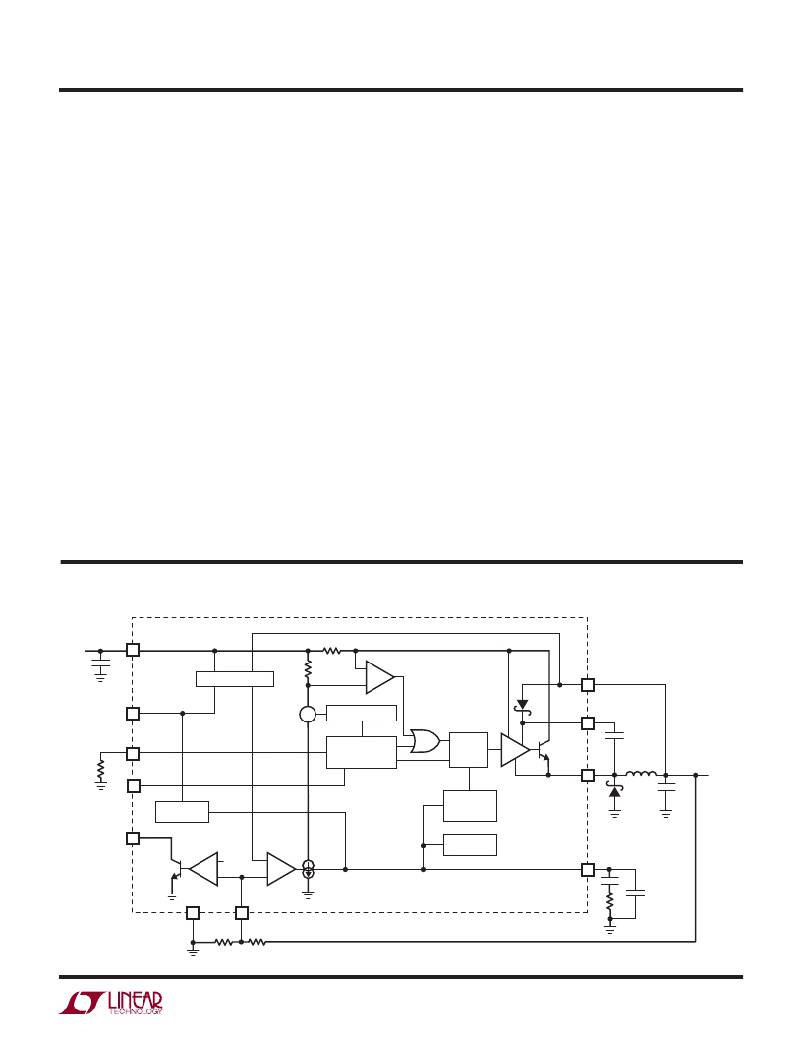
�BLOCK� DIAGRAM�
�V� IN�
�C1�
�4�
�V� IN�
�INTERNAL� 0.79V� REF�
�BD�
�1�
�5�
�RUN/SS�
�SLOPE� COMP�
�SWITCH�
�LATCH�
�BOOST�
�2�
�R� T�
�10�
�6�
�RT�
�SYNC�
�OSCILLATOR�
�200kHzTO2.4MHz�
�R�
�Q�
�S�
�DISABLE�
�Burst� Mode�
�SW�
�3�
�C3�
�D1�
�L1�
�C2�
�V� OUT�
�SOFT-START�
�DETECT�
�7�
�PG�
�ERROR� AMP�
�V� C� CLAMP�
�GND�
�+�
�–�
�0.725V�
�FB�
�+�
�–�
�V� C�
�9�
�C� C�
�R� C�
�C� F�
�11�
�R2�
�8�
�R1�
�3972� BD�
�3972fa�
�7�
�相关PDF资料 |
PDF描述 |
|---|---|
| GSC31DREF-S13 | CONN EDGECARD 62POS .100 EXTEND |
| MAX6716AUTRHD2+T | IC SUPERVISOR MPU SOT23-6 |
| GMC31DREF-S13 | CONN EDGECARD 62POS .100 EXTEND |
| MAX6716AUTRVD1+T | IC SUPERVISOR MPU SOT23-6 |
| RBC60DCMH | CONN EDGECARD 120POS .100 WW |
相关代理商/技术参数 |
参数描述 |
|---|---|
| LT3972IDD-TRPBF | 制造商:LINER 制造商全称:Linear Technology 功能描述:33V, 3.5A, 2.4MHz Step-Down Switching Regulator with 75μA Quiescent Current |
| LT3972IMSE#PBF | 功能描述:IC REG BUCK ADJ 3.5A 10MSOP RoHS:是 类别:集成电路 (IC) >> PMIC - 稳压器 - DC DC 开关稳压器 系列:- 设计资源:Design Support Tool 标准包装:1 系列:- 类型:升压(升压) 输出类型:固定 输出数:1 输出电压:3V 输入电压:0.75 V ~ 2 V PWM 型:- 频率 - 开关:- 电流 - 输出:100mA 同步整流器:是 工作温度:-40°C ~ 85°C 安装类型:表面贴装 封装/外壳:SOT-23-5 细型,TSOT-23-5 包装:剪切带 (CT) 供应商设备封装:TSOT-23-5 其它名称:AS1323-BTTT-30CT |
| LT3972IMSE#TRPBF | 功能描述:IC REG BUCK ADJ 3.5A 10MSOP RoHS:是 类别:集成电路 (IC) >> PMIC - 稳压器 - DC DC 开关稳压器 系列:- 设计资源:Design Support Tool 标准包装:1 系列:- 类型:升压(升压) 输出类型:固定 输出数:1 输出电压:3V 输入电压:0.75 V ~ 2 V PWM 型:- 频率 - 开关:- 电流 - 输出:100mA 同步整流器:是 工作温度:-40°C ~ 85°C 安装类型:表面贴装 封装/外壳:SOT-23-5 细型,TSOT-23-5 包装:剪切带 (CT) 供应商设备封装:TSOT-23-5 其它名称:AS1323-BTTT-30CT |
| LT3972IMSEPBF | 制造商:Linear Technology 功能描述:DC-DC Converter Step-Down 3.6-33V MSOP10 |
| LT3972IMSE-PBF | 制造商:LINER 制造商全称:Linear Technology 功能描述:33V, 3.5A, 2.4MHz Step-Down Switching Regulator with 75μA Quiescent Current |
发布紧急采购,3分钟左右您将得到回复。