参数资料
| 型号: | LT5554IUH#PBF |
| 厂商: | Linear Technology |
| 文件页数: | 11/32页 |
| 文件大小: | 0K |
| 描述: | IC VGA DIG CONTROL 32-QFN |
| 标准包装: | 73 |
| 应用: | 可变增益(VGA) |
| 电路数: | 1 |
| -3db带宽: | 1GHz |
| 电流 - 电源: | 200mA |
| 电压 - 电源,单路/双路(±): | 4.75 V ~ 5.25 V |
| 安装类型: | 表面贴装 |
| 封装/外壳: | 32-WFQFN 裸露焊盘 |
| 供应商设备封装: | 32-QFN 裸露焊盘(5x5) |
| 包装: | 管件 |
| 产品目录页面: | 1322 (CN2011-ZH PDF) |
第1页第2页第3页第4页第5页第6页第7页第8页第9页第10页当前第11页第12页第13页第14页第15页第16页第17页第18页第19页第20页第21页第22页第23页第24页第25页第26页第27页第28页第29页第30页第31页第32页
LT5554
19
5554f
APPLICATIONS INFORMATION
The differential outputs can also be converted to single-
ended 50Ω load using a center-tap transformer interface
shown in Figure 6 and Figure 16.
The internal 400Ω differential resistor (RO) sets the output
impedance and the maximum voltage gain (GMAX) to 36dB
when outputs OUT+, OUT– are open.
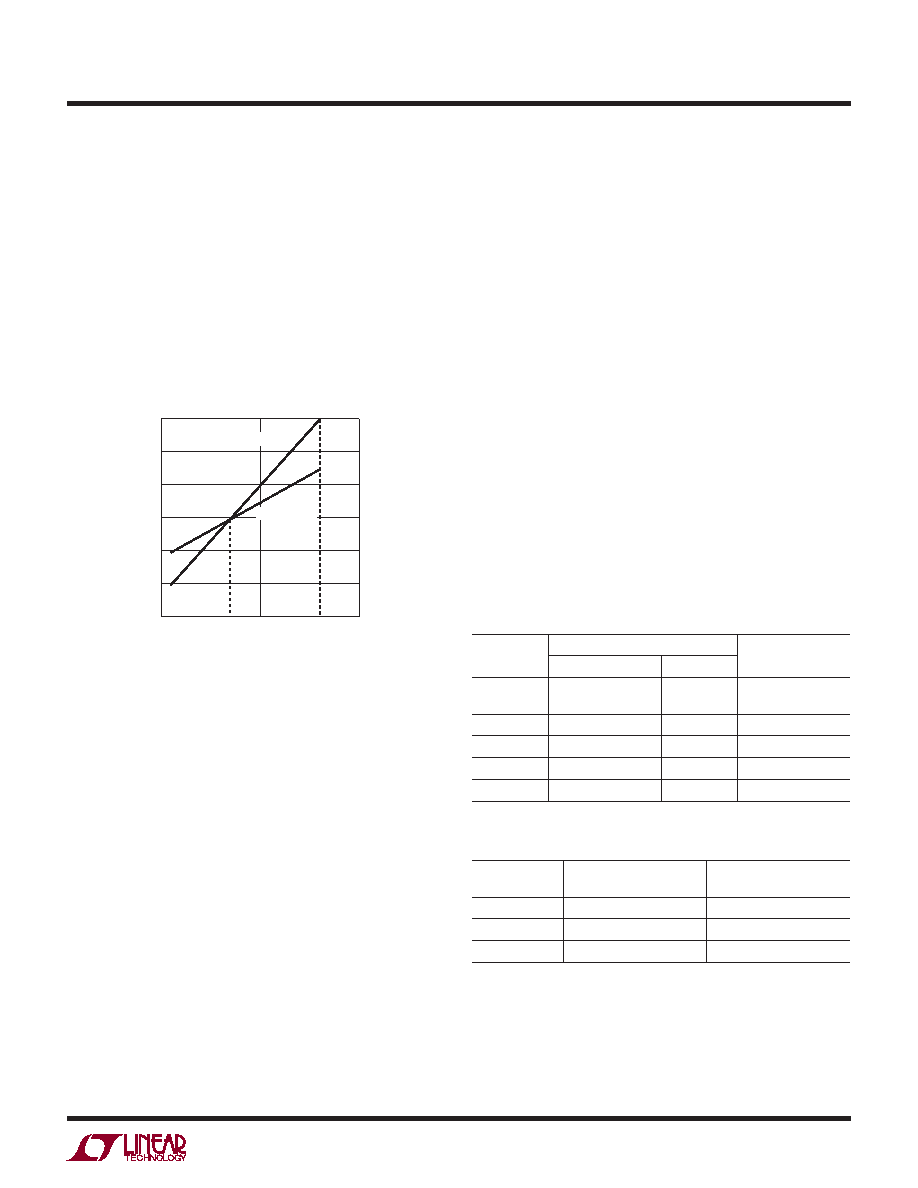
Figure 7 shows the Voltage and Power Gains as a func-
tion of ROUT, which is the total output loading at the open
collector amplier output including the internal resistor
RO = 400Ω.
Voltage clipping will occur with ROUT >140Ω, in which case
the instantaneous voltage at each OUT+ and OUT– outputs
is either <2V or >8V.
The output OP1dB = 20dBm can be achieved when ROUT =
130Ω. In this case, the LT5554 outputs reach both current
and voltage limiting for maximum output power.
Gain Control Interface
The MODE pin selects the interface to the LT5554 gain
control pins.
The PGx and STROBE control inputs can be congured
to be either DC-coupled (for TTL interface) or AC-coupled
(for ECL or low-voltage CMOS interfaces).
In addition, the STROBE input can be driven such that the
LT5554 gain state is updated asynchronously (PGx latch
control in transparent-mode) or controlled by positive
STROBE transition (PGx latch control in strobed-mode).
There are several options available for coupling type and
latch control which are given in the following tables:
Table1. MODE Input Options
MODE
(State)
COUPLING TYPE
PGx (Latch Control)
STROBE
PGx
LOW
AC Positive
Transition
AC
Strobe
OPEN
DC >2.2V
AC
Transparent
OPEN
0.6 to 2.2V
AC
Strobe
HIGH
DC >2.2V
DC
Transparent
HIGH
0.6 to 2.2V
DC
Strobe
Table2. MODE Input Levels
MODE
(State)
MODE
(Min Level)
MODE
(Max Level)
LOW
0
0.6V
OPEN
1.5V
2.5V
HIGH
VCC – 0.4V
VCC
Alternatively, the MODE pin can be left open (2V
internal).
Figure 7. Maximum Voltage and Power Gain vs ROUT
The gain vs ROUT relationship is given by the following
equations:
GV = 20log(GM ROUT) in dB
GP = 10log(RIN GM2 ROUT) in dB
Where RIN = 50Ω and GM = 0.15 siemens at GMAX
For wide band applications, the amplier bandwidth can
be extended by inductive peaking technique. The inductor
in series with the LT5554 outputs (OUT+ OUT–) can have
a value up to some tens of nH depending on ROUT value
and board capacitance.
The current limiting will occur with ROUT <140Ω, in which
case the instantaneous signal current at the output exceeds
IODC = 45mA.
ROUT (Ω)
10
MAXIMUM
GAIN
(dB)
36
30
24
18
12
6
0
100
400
50
5554 F07
1000
VOLTAGE GAIN
POWER GAIN
相关PDF资料 |
PDF描述 |
|---|---|
| 2-1877846-1 | PLUG 6POS 0 DEG GRY/RED 2.7-3.9 |
| VI-B3J-MU-F2 | CONVERTER MOD DC/DC 36V 200W |
| 1-1877846-5 | PLUG 6POS 0 DEG BLK/RED 2.7-3.9 |
| 1-1877846-2 | PLUG 6POS 80 DEG GRY/GRY 2.7-3.9 |
| VI-B3H-MU-F4 | CONVERTER MOD DC/DC 52V 200W |
相关代理商/技术参数 |
参数描述 |
|---|---|
| LT5554IUH-TRPBF | 制造商:LINER 制造商全称:Linear Technology 功能描述:Broadband Ultra Low Distortion 7-Bit Digitally Controlled VGA |
| LT5557 | 制造商:LINER 制造商全称:Linear Technology 功能描述:4GHz to 6GHz High Dynamic Range Downconverting Mixer |
| LT5557EUF#PBF | 功能描述:IC DOWNCONVERTING MIXER 16-QFN RoHS:是 类别:RF/IF 和 RFID >> RF 混频器 系列:LT5557 产品培训模块:Lead (SnPb) Finish for COTS Obsolescence Mitigation Program 标准包装:100 系列:- RF 型:W-CDMA 频率:2.11GHz ~ 2.17GHz 混频器数目:1 增益:17dB 噪音数据:2.2dB 次要属性:- 电流 - 电源:11.7mA 电源电压:2.7 V ~ 3.3 V 包装:托盘 封装/外壳:12-VFQFN 裸露焊盘 供应商设备封装:12-QFN-EP(3x3) |
| LT5557EUF#TRPBF | 功能描述:IC DOWNCONVERTING MIXER 16-QFN RoHS:是 类别:RF/IF 和 RFID >> RF 混频器 系列:LT5557 产品培训模块:Lead (SnPb) Finish for COTS Obsolescence Mitigation Program 标准包装:100 系列:- RF 型:W-CDMA 频率:2.11GHz ~ 2.17GHz 混频器数目:1 增益:17dB 噪音数据:2.2dB 次要属性:- 电流 - 电源:11.7mA 电源电压:2.7 V ~ 3.3 V 包装:托盘 封装/外壳:12-VFQFN 裸露焊盘 供应商设备封装:12-QFN-EP(3x3) |
| LT5557EUFPBF | 制造商:Linear Technology 功能描述:0.4-3.8GHz 3.3V Active Down Mixer QFN16 |
发布紧急采购,3分钟左右您将得到回复。