- 您现在的位置:买卖IC网 > PDF目录2156 > LT6402CUD-20#TRPBF (Linear Technology)IC DIFF AMP/ADC DRVR 16-QFN PDF资料下载
参数资料
| 型号: | LT6402CUD-20#TRPBF |
| 厂商: | Linear Technology |
| 文件页数: | 5/16页 |
| 文件大小: | 0K |
| 描述: | IC DIFF AMP/ADC DRVR 16-QFN |
| 标准包装: | 2,500 |
| 放大器类型: | 差分 |
| 电路数: | 2 |
| 输出类型: | 差分 |
| 转换速率: | 400 V/µs |
| -3db带宽: | 300MHz |
| 电流 - 输入偏压: | 5µA |
| 电压 - 输入偏移: | 1000µV |
| 电流 - 电源: | 30mA |
| 电流 - 输出 / 通道: | 35mA |
| 电压 - 电源,单路/双路(±): | 4 V ~ 5.5 V,±2 V ~ 2.5 V |
| 工作温度: | 0°C ~ 70°C |
| 安装类型: | 表面贴装 |
| 封装/外壳: | 16-WFQFN 裸露焊盘 |
| 供应商设备封装: | 16-QFN-EP(3x3) |
| 包装: | 带卷 (TR) |
13
640220fa
LT6402-20
APPLICATIO S I FOR ATIO
WU
U
solution of 14pF from each ltered output to ground plus
a 14pF capacitor between the ltered outputs would also
halve the lter bandwidth (Figure 7).
Bandpass ltering is also easily implemented with just a
few external components. An additional 560pF and 62nH,
each added differentially between +OUTFILTERED and
–OUTFILTERED creates a bandpass lter with a 26MHz
center frequency, –3dB points of 23MHz and 30MHz, and
1.6dB of insertion loss (Figure 8).
Output Common Mode Adjustment
The LT6402-20’s output common mode voltage is set by
the VOCM pin. It is a high-impedance input, capable of
setting the output common mode voltage anywhere in
a range from 1.1V to 3.6V. Bandwidth of the VOCM pin is
typically 200MHz, so for applications where the VOCM pin
is tied to a DC bias voltage, a 0.1F capacitor at this pin is
recommended. For best distortion performance, the voltage
at the VOCM pin should be between 1.8V and 2.6V.
When interfacing with most ADCs, there is generally a
VOCM output pin that is at about half of the supply voltage
of the ADC. For 5V ADCs such as the LTC17XX family, this
VOCM output pin should be connected directly (with the
addition of a 0.1F capacitor) to the input VOCM pin of the
LT6402-20. For 3V ADCs such as the LTC22XX families,
the LT6402-20 will function properly using the 1.65V from
the ADC’s VCM reference pin, but improved Spurious Free
Dynamic Range (SFDR) and distortion performance can
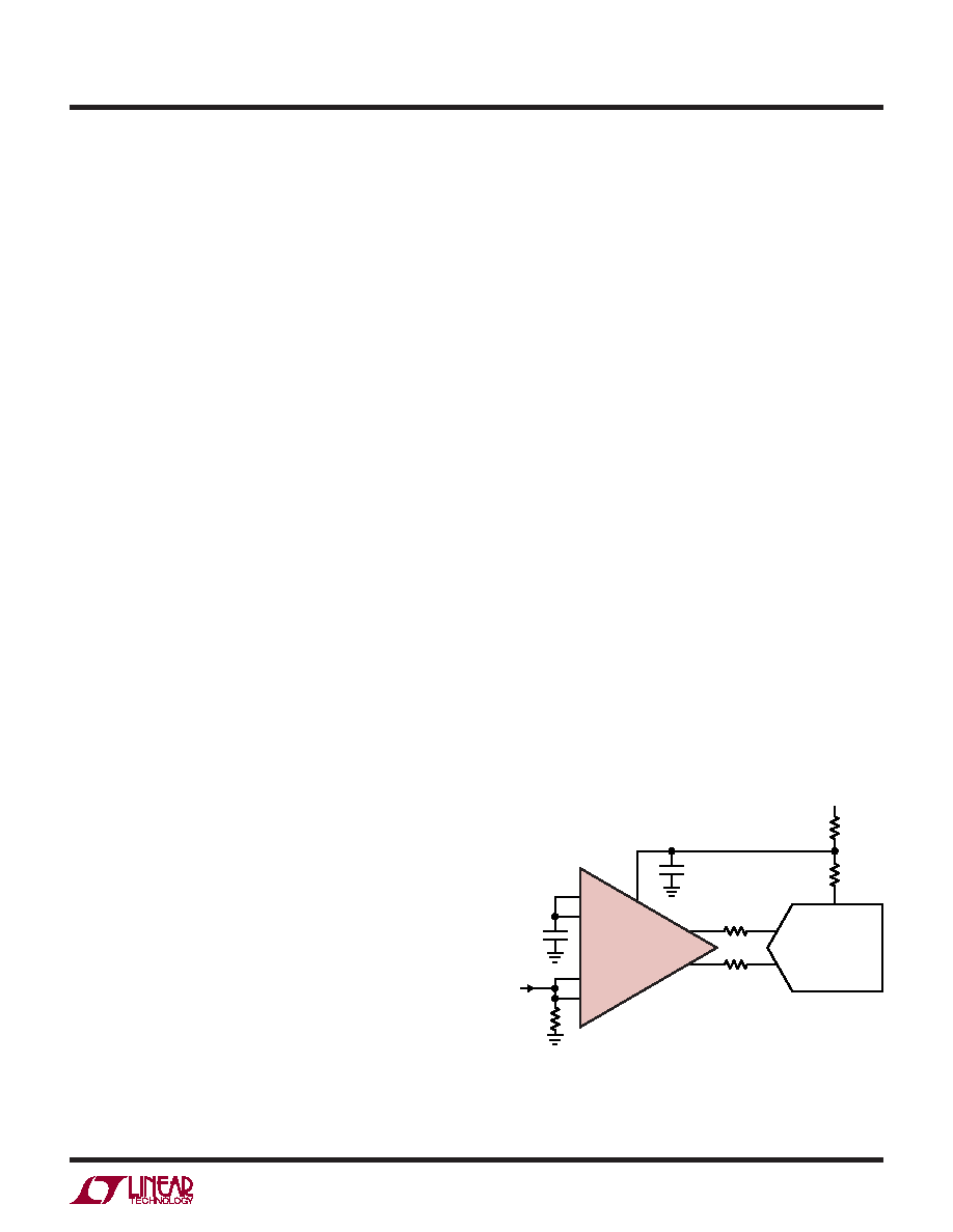
be achieved by level-shifting the LTC22XX’s VCM reference
voltage up to at least 1.8V. This can be accomplished as
shown in Figure 9 by using a resistor divider between the
LTC22XX’s VCM output pin and VCC and then bypassing
the LT6402-20’s VOCM pin with a 0.1F capacitor. For a
common mode voltage above 1.9V, AC coupling capacitors
are recommended between the LT6402-20 and LTC22XX
ADCs because of the input voltage range constraints of
the ADC.
Large Output Voltage Swings
The LT6402-20 has been designed to provide the
3.2VP-P output swing needed by the LTC1748 family
of 14-bit low-noise ADCs. This additional output swing
improves system SNR by up to 4dB.
Input Bias Voltage and Bias Current
The input pins of the LT6402-20 are internally biased to
the voltage applied to the VOCM pin. No external biasing
resistors are needed, even for AC-coupled operation. The
input bias current is determined by the voltage difference
between the input common mode voltage and the VOCM
pin (which sets the output common mode voltage). For
example, if the inputs are tied to 2.5V with the VOCM pin
at 2.2V, then a total input bias current of 1mA will ow
into the LT6402-20’s +INA and +INB pins. Furthermore,
an additional input bias current totaling 1mA will ow into
the –INA and –INB inputs.
Application (Demo) Boards
The DC954A Demo Board has been created for stand-alone
evaluation of the LT6402-20 with either single-ended or
differential input and output signals. As shown, it accepts
a single-ended input and produces a single-ended output
so that the LT6402-20 can be evaluated using standard
laboratory test equipment. For more information on this
Demo Board, please refer to the layout and schematic
diagrams found later in this data sheet.
There are also additional demo boards available that
combine the LT6402-20 with a variety of different Linear
Technology ADCs. Please contact the factory for more
information on these demo boards.
6402 F9
IF IN
LT6402-20
–INA
–INB
VOCM
2
31
6
7
1
2
+INB
+INA
14
13
15
121
16
10
10
LTC22xx
0.1
F
0.1
F
+OUTFILTERED
–OUTFILTERED
AIN+
AIN–
4.02k
11k
1.9V
1.5V
3V
VCM
Figure 9. Level Shifting 3V ADC VCM Voltage for
Improved SFDR
相关PDF资料 |
PDF描述 |
|---|---|
| LT6402CUD-6#PBF | IC DIFF AMP/ADC DVR 6DB 16-QFN |
| LT6411CUD#TRPBF | IC ADC DRVR/GAIN AMP 16-QFN |
| LT6600CS8-15#TRPBF | IC AMP DIFF LP FLTR 15MHZ 8-SOIC |
| LT6600CS8-5#TRPBF | IC AMP DIFF LP FLTR 5MHZ 8-SOIC |
| LT6600IS8-10 | IC AMP DIFF 10MHZ LP FLTR 8-SOIC |
相关代理商/技术参数 |
参数描述 |
|---|---|
| LT6402CUD-6 | 制造商:LINER 制造商全称:Linear Technology 功能描述:300MHz Low Distortion, Low Noise Differential Amplifi er/ ADC Driver (AV = 6dB) |
| LT6402CUD-6#PBF | 功能描述:IC DIFF AMP/ADC DVR 6DB 16-QFN RoHS:是 类别:集成电路 (IC) >> Linear - Amplifiers - Instrumentation 系列:- 其它有关文件:Automotive Product Guide 产品培训模块:Lead (SnPb) Finish for COTS Obsolescence Mitigation Program 标准包装:1 系列:- 放大器类型:通用 电路数:1 输出类型:满摆幅 转换速率:3 V/µs 增益带宽积:10MHz -3db带宽:- 电流 - 输入偏压:1pA 电压 - 输入偏移:70µV 电流 - 电源:2.5mA 电流 - 输出 / 通道:48mA 电压 - 电源,单路/双路(±):2.7 V ~ 5.5 V,±1.35 V ~ 2.75 V 工作温度:-40°C ~ 125°C 安装类型:表面贴装 封装/外壳:SOT-23-6 供应商设备封装:SOT-6 包装:Digi-Reel® 其它名称:MAX4475AUT#TG16DKR |
| LT6402CUD-6#TRPBF | 功能描述:IC DIFF AMP/ADC DVR 6DB 16-QFN RoHS:是 类别:集成电路 (IC) >> Linear - Amplifiers - Instrumentation 系列:- 产品培训模块:Lead (SnPb) Finish for COTS Obsolescence Mitigation Program 标准包装:1 系列:- 放大器类型:电流检测 电路数:1 输出类型:- 转换速率:- 增益带宽积:125kHz -3db带宽:- 电流 - 输入偏压:- 电压 - 输入偏移:100µV 电流 - 电源:1.1µA 电流 - 输出 / 通道:- 电压 - 电源,单路/双路(±):- 工作温度:-40°C ~ 85°C 安装类型:表面贴装 封装/外壳:4-WFBGA,CSPBGA 供应商设备封装:4-UCSP(2x2) 包装:剪切带 (CT) 其它名称:MAX9634WERS+TCT |
| LT6402CUD-6-PBF | 制造商:LINER 制造商全称:Linear Technology 功能描述:300MHz Low Distortion, Low Noise Differential Amplifi er/ ADC Driver (AV = 6dB) |
| LT6402CUD-6-TR | 制造商:LINER 制造商全称:Linear Technology 功能描述:300MHz Low Distortion, Low Noise Differential Amplifi er/ ADC Driver (AV = 6dB) |
发布紧急采购,3分钟左右您将得到回复。