参数资料
| 型号: | LT6604CUFF-2.5#PBF |
| 厂商: | Linear Technology |
| 文件页数: | 3/16页 |
| 文件大小: | 0K |
| 描述: | IC AMP DIFF LN DUAL 34-QFN |
| 标准包装: | 52 |
| 放大器类型: | 差分 |
| 电路数: | 2 |
| 输出类型: | 差分 |
| 电流 - 输入偏压: | 15µA |
| 电压 - 输入偏移: | 5000µV |
| 电流 - 电源: | 28mA |
| 电压 - 电源,单路/双路(±): | 3 V ~ 11 V,±1.5 V ~ 5.5 V |
| 工作温度: | 0°C ~ 70°C |
| 安装类型: | 表面贴装 |
| 封装/外壳: | 34-WFQFN 裸露焊盘 |
| 供应商设备封装: | 34-QFN-EP(4x7) |
| 包装: | 管件 |
LT6604-2.5
11
660425fa
APPLICATIONS INFORMATION
VOCM can be shorted to VMID for simplicity. If a different
common mode output voltage is required, connect VOCM
to a voltage source or resistor network. For 3V and 3.3V
supplies the voltage at VOCM must be less than or equal
to the mid supply level. For example, voltage (VOCM) ≤
1.65V on a single 3.3V supply. For power supply voltages
higher than 3.3V the voltage at VOCM can be set above mid
supply, as shown in Table 1. The voltage on VOCM should
not be more than 1V below the voltage on VMID. VOCM is
a high impedance input.
Table 1. Output Common Mode Range for Various Supplies
SUPPLY
VOLTAGE
DIFFERENTIAL OUT
VOLTAGE SWING
OUTPUT COMMON MODE RANGE
FOR LOW DISTORTION
3V
4VP-P
2VP-P
1VP-P
1.4V ≤ VOCM ≤ 1.6V
1V ≤ VOCM ≤ 1.6V
0.75V ≤ VOCM ≤ 1.6V
5V
8VP-P
4VP-P
2VP-P
1VP-P
2.4V ≤ VOCM ≤ 2.6V
1.5V ≤ VOCM ≤ 3.5V
1V ≤ VOCM ≤ 3.75V
0.75V ≤ VOCM ≤ 3.75V
±5V
9VP-P
4VP-P
2VP-P
1VP-P
–2V ≤ VOCM ≤ 2V
–3.5V ≤ VOCM ≤ 3.5V
–3.75V ≤ VOCM ≤ 3.75V
–4.25V ≤ VOCM ≤ 3.75V
NOTE: The voltage at VOCM should not be more than 1V below the voltage
at VMID. To achieve some of the output common mode ranges shown in the
table, the voltage at VMID must be set externally to a value below mid supply.
The LT6604-2.5 was designed to process a variety of
input signals including signals centered on the mid-sup-
ply voltage and signals that swing between ground and
a positive voltage in a single supply system (Figure 1).
The allowable range of the input common mode voltage
(the average of VIN+ and VIN– in Figure 1) is determined
by the power supply level and gain setting (see “Electrical
Characteristics”).
Common Mode DC Currents
In applications like Figure 1 and Figure 3 where the LT6604-
2.5 not only provides lowpass ltering but also level shifts
the common mode voltage of the input signal, DC currents
will be generated through the DC path between input and
output terminals. Minimize these currents to decrease
power dissipation and distortion.
Consider the application in Figure 3. VMID sets the output
common mode voltage of the 1st differential amplier inside
the LT6604-2.5 channel (see the “Block Diagram” section)
at 2.5V. Since the input common mode voltage is near 0V,
there will be approximately a total of 2.5V drop across
the series combination of the internal 1580Ω feedback
resistor and the external 402Ω input resistor. The result-
ing 1.25mA common mode DC current in each input path,
must be absorbed by the sources VIN+ and VIN–. VOCM sets
the common mode output voltage of the 2nd differential
amplier inside the LT6604-2.5 channel, and therefore sets
the common mode output voltage of the lter. Since, in
the example of Figure 3, VOCM differs from VMID by 0.5V,
an additional 625μA (312μA per side) of DC current will
ow in the resistors coupling the 1st differential amplier
output stage to the lter output. Thus, a total of 3.125mA
is used to translate the common mode voltages.
A simple modication to Figure 3 will reduce the DC com-
mon mode currents by 36%. If VMID is shorted to VOCM
the common mode output voltage of both op amp stages
will be 2V and the resulting DC current will be 2mA. Of
course, by AC-coupling the inputs of Figure 3, the common
mode DC current can be reduced to 625μA.
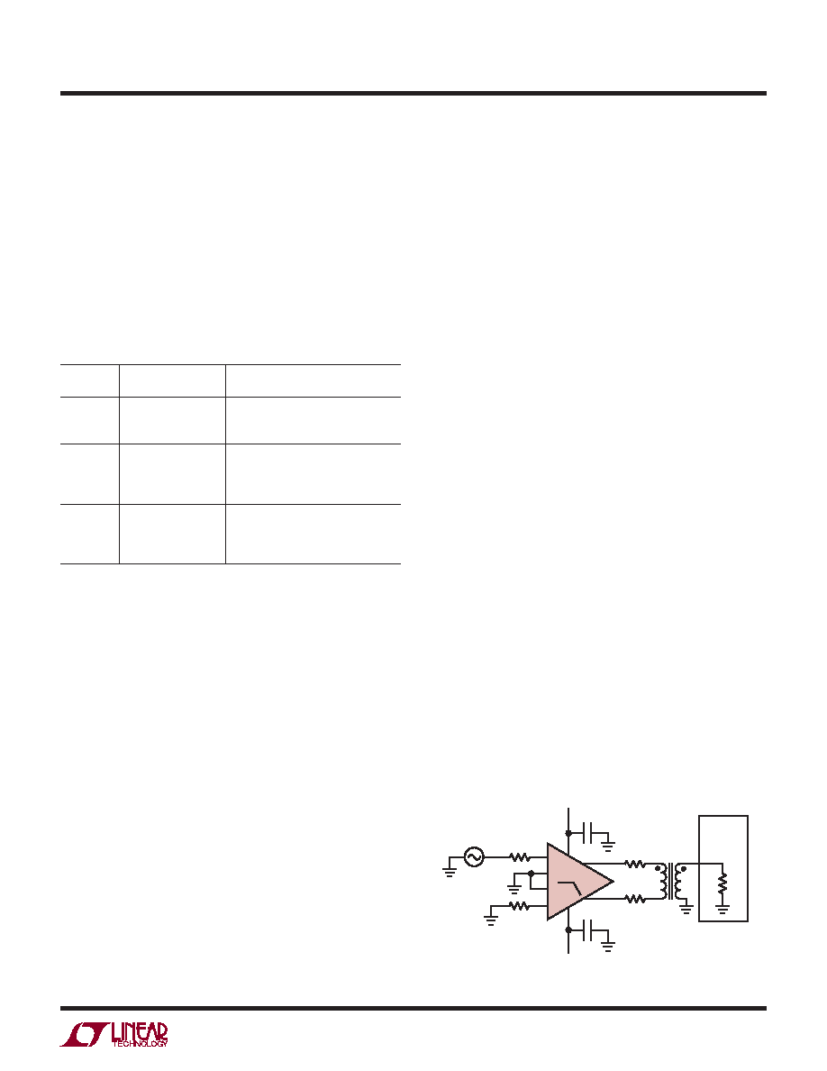
Noise
The noise performance of the LT6604-2.5 channel can be
evaluated with the circuit of Figure 6. Given the low noise
output of the LT6604-2.5 and the 6dB attenuation of the
transformer coupling network, it is necessary to measure
the noise oor of the spectrum analyzer and subtract the
instrument noise from the lter noise measurement.
Example: With the IC removed and the 25Ω resistors
grounded, Figure 6, measure the total integrated noise (eS)
of the spectrum analyzer from 10kHz to 2.5MHz. With the
IC inserted, the signal source (VIN) disconnected, and the
Figure 6
–
+
0.1μF
2.5V
–2.5V
–
+
1/2
LT6604-2.5
RIN
25Ω
660425 F06
SPECTRUM
ANALYZER
INPUT
50Ω
VIN
COILCRAFT
TTWB-1010
1:1
25
27
4
34
6
2
29
7
相关PDF资料 |
PDF描述 |
|---|---|
| 2-172076-6 | CONN RCPT HSG 1POS .250 BLUE |
| 2-172076-2 | CONN RCPT HSG 1POS .250 BLACK |
| 8-154719-4 | CONN RCPT HSG 1POS .250 NATURAL |
| 0001.2029 | FUSE 40A 500V BLK DT III |
| 2036-25-C2FLF | GAS DISCHARGE TUBE |
相关代理商/技术参数 |
参数描述 |
|---|---|
| LT6604CUFF-5#PBF | 功能描述:IC AMP DIFF LN DUAL 34-QFN RoHS:是 类别:集成电路 (IC) >> Linear - Amplifiers - Instrumentation 系列:- 标准包装:2,500 系列:Excalibur™ 放大器类型:J-FET 电路数:1 输出类型:- 转换速率:45 V/µs 增益带宽积:10MHz -3db带宽:- 电流 - 输入偏压:20pA 电压 - 输入偏移:490µV 电流 - 电源:1.7mA 电流 - 输出 / 通道:48mA 电压 - 电源,单路/双路(±):4.5 V ~ 38 V,±2.25 V ~ 19 V 工作温度:-40°C ~ 85°C 安装类型:表面贴装 封装/外壳:8-SOIC(0.154",3.90mm 宽) 供应商设备封装:8-SOIC 包装:带卷 (TR) |
| LT6604CUFF-5#TRPBF | 功能描述:IC AMP DIFF LN DUAL 34-QFN RoHS:是 类别:集成电路 (IC) >> Linear - Amplifiers - Instrumentation 系列:- 标准包装:2,500 系列:Excalibur™ 放大器类型:J-FET 电路数:1 输出类型:- 转换速率:45 V/µs 增益带宽积:10MHz -3db带宽:- 电流 - 输入偏压:20pA 电压 - 输入偏移:490µV 电流 - 电源:1.7mA 电流 - 输出 / 通道:48mA 电压 - 电源,单路/双路(±):4.5 V ~ 38 V,±2.25 V ~ 19 V 工作温度:-40°C ~ 85°C 安装类型:表面贴装 封装/外壳:8-SOIC(0.154",3.90mm 宽) 供应商设备封装:8-SOIC 包装:带卷 (TR) |
| LT6604CUFF-5-PBF | 制造商:LINER 制造商全称:Linear Technology 功能描述:Dual Very Low Noise, Differential Amplifi er and 5MHz Lowpass Filter |
| LT6604CUFF-5-TRPBF | 制造商:LINER 制造商全称:Linear Technology 功能描述:Dual Very Low Noise, Differential Amplifi er and 5MHz Lowpass Filter |
| LT6604IUFF-10#PBF | 功能描述:IC AMP DIFF LN DUAL 34-QFN RoHS:是 类别:集成电路 (IC) >> Linear - Amplifiers - Instrumentation 系列:- 标准包装:2,500 系列:- 放大器类型:通用 电路数:4 输出类型:- 转换速率:0.6 V/µs 增益带宽积:1MHz -3db带宽:- 电流 - 输入偏压:45nA 电压 - 输入偏移:2000µV 电流 - 电源:1.4mA 电流 - 输出 / 通道:40mA 电压 - 电源,单路/双路(±):3 V ~ 32 V,±1.5 V ~ 16 V 工作温度:0°C ~ 70°C 安装类型:表面贴装 封装/外壳:14-TSSOP(0.173",4.40mm 宽) 供应商设备封装:14-TSSOP 包装:带卷 (TR) 其它名称:LM324ADTBR2G-NDLM324ADTBR2GOSTR |
发布紧急采购,3分钟左右您将得到回复。