参数资料
| 型号: | LT6604CUFF-2.5#PBF |
| 厂商: | Linear Technology |
| 文件页数: | 4/16页 |
| 文件大小: | 0K |
| 描述: | IC AMP DIFF LN DUAL 34-QFN |
| 标准包装: | 52 |
| 放大器类型: | 差分 |
| 电路数: | 2 |
| 输出类型: | 差分 |
| 电流 - 输入偏压: | 15µA |
| 电压 - 输入偏移: | 5000µV |
| 电流 - 电源: | 28mA |
| 电压 - 电源,单路/双路(±): | 3 V ~ 11 V,±1.5 V ~ 5.5 V |
| 工作温度: | 0°C ~ 70°C |
| 安装类型: | 表面贴装 |
| 封装/外壳: | 34-WFQFN 裸露焊盘 |
| 供应商设备封装: | 34-QFN-EP(4x7) |
| 包装: | 管件 |
LT6604-2.5
12
660425fa
APPLICATIONS INFORMATION
input resistors grounded, measure the total integrated noise
out of the lter (eO). With the signal source connected, set
the frequency to 100kHz and adjust the amplitude until
VIN measures 100mVP-P. Measure the output amplitude,
VOUT, and compute the passband gain A = VOUT/VIN. Now
compute the input referred integrated noise (eIN) as:
e
ee
A
IN
OS
=
() – (
)
22
Table 2 lists the typical input referred integrated noise for
various values of RIN.
Table 2. Noise Performance
PASSBAND
GAIN
RIN
INPUT REFERRED
INTEGRATED NOISE
10kHz TO 2.5MHz
INPUT REFERRED
INTEGRATED NOISE
10kHz TO 5MHz
4
402Ω
18μVRMS
23μVRMS
2
806Ω
29μVRMS
39μVRMS
1
1580Ω
51μVRMS
73μVRMS
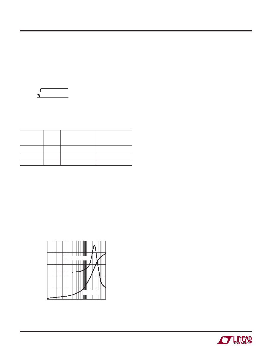
Figure 7 is plot of the noise spectral density as a function
of frequency for an LT6604-2.5 channel with RIN = 1580Ω
using the xture of Figure 6 (the instrument noise has
been subtracted from the results).
The noise at each output is comprised of a differential
component and a common mode component. Using a
transformer or combiner to convert the differential outputs
to single-ended signal rejects the common mode noise and
gives a true measure of the S/N achievable in the system.
Conversely, if each output is measured individually and the
noise power added together, the resulting calculated noise
level will be higher than the true differential noise.
Power Dissipation
The LT6604-2.5 ampliers combine high speed with large
signal currents in a small package. There is a need to en-
sure that the die’s junction temperature does not exceed
150°C. The LT6604-2.5 has an exposed pad (pin 35) which
is connected to the negative supply (V–). Connecting the
pad to a ground plane helps to dissipate the heat generated
by the chip. Metal trace and plated through-holes can be
used to spread the heat generated by the device to the
backside of the PC board.
Junction temperature, TJ, is calculated from the ambient
temperature, TA, and power dissipation, PD. The power
dissipation is the product of supply voltage, VS, and total
supply current, IS. Therefore, the junction temperature is
given by:
TJ = TA + (PD θJA) = TA + (VS IS θJA)
where the supply current, IS, is a function of signal level,
load impedance, temperature and common mode voltages.
For a given supply voltage, the worst-case power dissipation
occurs when the differential input signal is maximum, the
common mode currents are maximum (see Applications
Information regarding Common Mode DC Currents), the
load impedance is small and the ambient temperature is
maximum. To compute the junction temperature, measure
the supply current under these worst-case conditions, use
43°C/W as the package thermal resistance, then apply the
equation for TJ. For example, using the circuit in Figure 3
with DC differential input voltage of 1V, a differential
output voltage of 4V, no load resistance and an ambient
temperature of 85°C, the supply current (current into V+)
measures 37.6mA per channel. The resulting junction
temperature is: TJ = TA + (PD θJA) = 85 + (5 2 0.0376
43) = 101°C. The thermal resistance can be affected by
the amount of copper on the PCB that is connected to V–.
The thermal resistance of the circuit can increase if the
Exposed Pad is not connected to a large ground plane
with a number of vias.
FREQUENCY (MHz)
0.01
0
30
40
50
0.1
1
10
660425 F07
20
10
0
60
80
100
40
20
NOISE
SPECTRAL
DENSIT
Y
(nV
RMS
/√
Hz
)
INTEGRA
TED
NOISE
(μ
V
RMS
)
SPECTRAL DENSITY
INTEGRATED
Figure 7. Input Referred Noise, Gain = 1
相关PDF资料 |
PDF描述 |
|---|---|
| 2-172076-6 | CONN RCPT HSG 1POS .250 BLUE |
| 2-172076-2 | CONN RCPT HSG 1POS .250 BLACK |
| 8-154719-4 | CONN RCPT HSG 1POS .250 NATURAL |
| 0001.2029 | FUSE 40A 500V BLK DT III |
| 2036-25-C2FLF | GAS DISCHARGE TUBE |
相关代理商/技术参数 |
参数描述 |
|---|---|
| LT6604CUFF-5#PBF | 功能描述:IC AMP DIFF LN DUAL 34-QFN RoHS:是 类别:集成电路 (IC) >> Linear - Amplifiers - Instrumentation 系列:- 标准包装:2,500 系列:Excalibur™ 放大器类型:J-FET 电路数:1 输出类型:- 转换速率:45 V/µs 增益带宽积:10MHz -3db带宽:- 电流 - 输入偏压:20pA 电压 - 输入偏移:490µV 电流 - 电源:1.7mA 电流 - 输出 / 通道:48mA 电压 - 电源,单路/双路(±):4.5 V ~ 38 V,±2.25 V ~ 19 V 工作温度:-40°C ~ 85°C 安装类型:表面贴装 封装/外壳:8-SOIC(0.154",3.90mm 宽) 供应商设备封装:8-SOIC 包装:带卷 (TR) |
| LT6604CUFF-5#TRPBF | 功能描述:IC AMP DIFF LN DUAL 34-QFN RoHS:是 类别:集成电路 (IC) >> Linear - Amplifiers - Instrumentation 系列:- 标准包装:2,500 系列:Excalibur™ 放大器类型:J-FET 电路数:1 输出类型:- 转换速率:45 V/µs 增益带宽积:10MHz -3db带宽:- 电流 - 输入偏压:20pA 电压 - 输入偏移:490µV 电流 - 电源:1.7mA 电流 - 输出 / 通道:48mA 电压 - 电源,单路/双路(±):4.5 V ~ 38 V,±2.25 V ~ 19 V 工作温度:-40°C ~ 85°C 安装类型:表面贴装 封装/外壳:8-SOIC(0.154",3.90mm 宽) 供应商设备封装:8-SOIC 包装:带卷 (TR) |
| LT6604CUFF-5-PBF | 制造商:LINER 制造商全称:Linear Technology 功能描述:Dual Very Low Noise, Differential Amplifi er and 5MHz Lowpass Filter |
| LT6604CUFF-5-TRPBF | 制造商:LINER 制造商全称:Linear Technology 功能描述:Dual Very Low Noise, Differential Amplifi er and 5MHz Lowpass Filter |
| LT6604IUFF-10#PBF | 功能描述:IC AMP DIFF LN DUAL 34-QFN RoHS:是 类别:集成电路 (IC) >> Linear - Amplifiers - Instrumentation 系列:- 标准包装:2,500 系列:- 放大器类型:通用 电路数:4 输出类型:- 转换速率:0.6 V/µs 增益带宽积:1MHz -3db带宽:- 电流 - 输入偏压:45nA 电压 - 输入偏移:2000µV 电流 - 电源:1.4mA 电流 - 输出 / 通道:40mA 电压 - 电源,单路/双路(±):3 V ~ 32 V,±1.5 V ~ 16 V 工作温度:0°C ~ 70°C 安装类型:表面贴装 封装/外壳:14-TSSOP(0.173",4.40mm 宽) 供应商设备封装:14-TSSOP 包装:带卷 (TR) 其它名称:LM324ADTBR2G-NDLM324ADTBR2GOSTR |
发布紧急采购,3分钟左右您将得到回复。