参数资料
| 型号: | LTC1052CSW#TR |
| 厂商: | Linear Technology |
| 文件页数: | 4/24页 |
| 文件大小: | 0K |
| 描述: | IC OPAMP CHOP STABLE LN 16SOIC |
| 标准包装: | 1,000 |
| 系列: | LTCMOS™ |
| 放大器类型: | 断路器(零漂移) |
| 电路数: | 1 |
| 转换速率: | 4 V/µs |
| 增益带宽积: | 1.2MHz |
| 电流 - 输入偏压: | 1pA |
| 电压 - 输入偏移: | 0.5µV |
| 电流 - 电源: | 1.7mA |
| 电压 - 电源,单路/双路(±): | 4.75 V ~ 16 V,±2.38 V ~ 8 V |
| 工作温度: | 0°C ~ 70°C |
| 安装类型: | 表面贴装 |
| 封装/外壳: | 16-SOIC(0.295",7.50mm 宽) |
| 供应商设备封装: | 16-SO |
| 包装: | 带卷 (TR) |
LTC1052/LTC7652
12
1052fa
OUTPUT CLAMP
If the LTC1052 is driven into saturation, the nulling loop,
attempting to force the differential input voltage to zero,
will drive CEXTA and CEXTB to a supply rail. After the
saturating drive is removed, the capacitors take a finite
time to recover—this is the overload recovery time. The
overload recovery is longest when the capacitors are
driven to the negative rail (refer to Overload Recovery in
the Typical Performance Characteristics section). The
overload recovery time in this case is typically 225ms. In
the opposite direction (i.e., CEXTA and CEXTB at positive
rail), it is about ten times faster (25ms). The overload
recovery time for the LTC1052 is much faster than com-
petitive devices; however, if a faster overload recovery
time is necessary, the output clamp function can be used.
When the output clamp is connected to the negative input
it prevents the amplifier from saturating, thus keeping
CEXTA and CEXTB at their nominal voltages. The output
clamp is a switch that turns on when the output gets to
APPLICATIO S I FOR ATIO
WU
UU
within approximately 1V of either supply rail. This switch
is in parallel with the amplifier’s feedback resistor. As the
output moves closer to the rail, the switch on
resistance decreases, reducing the closed loop gain. The
output swing is reduced when the clamp function is used.
How much current the output clamp leaks when off
is important because, when used, it is connected to the
amplifier’s negative input. Any current acts like input bias
current and will degrade accuracy. At the other extreme,
the maximum current the clamp conducts when on deter-
mines how much overdrive the clamp will take, and still
keep the amplifier from saturating. Both of these numbers
are guaranteed in the Electrical Characteristics section.
LOW SUPPLY OPERATION
The minimum supply voltage for proper operation of the
LTC1052 is typically 4.0V (±2.0V). In single supply
applications, PSRR is guaranteed down to 4.7V (±2.35V).
This assures proper operation down to the minimum TTL
specified voltage of 4.75V.
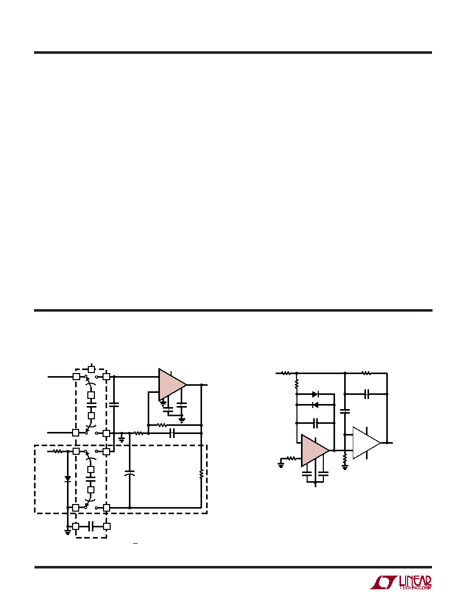
TYPICAL APPLICATIO S
U
5V Powered Ultraprecision Instrumentation Amplifier
Fast Precision Inverter
LTC1052/7652 TA04
8pF
–5V
1N4148
10k*
1000pF
5V
300pF
7
0.1F
*1% METAL FILM
INPUT
0.1F
2
3
10k
–5V
OUTPUT
4
6
10k
2
6
8
4
1
10k
7
3
FULL POWER BANDWIDTH = 2MHz
SLEW RATE = 40V/s
SETTLING (10V STEP) = 12s TO 0.01%
BIAS CURRENT DC = 30pA
OFFSET DRIFT = 50nV/°C
OFFSET VOLTAGE = 5V
10k*
+
–
LT318A
+
–
LTC1052
LTC1052/7652 TA03
6
C2
+IN
VOUT
5V
0.1F
LTC1043
C1
43k
0.22F
R2
100k
–IN
1N914
0.0047F
5V
7
R1
100
≈ – 0.5V
CIRCUITRY WITHIN DASHED LINES MAY BE DELETED IF OUTPUT
DOES NOT HAVE TO SWING ALL THE WAY TO GROUND
1F
15
12
4
7
13
C3
1F
C4
1F
5
16
17
18
3
2
8
3
2
4
0.1F
1
10k
DRIFT = 50nV/°C
VOS = 3V
GAIN =
CMRR = >120dB DC – 20kHz
BANDWIDTH = 10Hz
R2
R1
+ 1
8
+
–
LTC1052
11
14
6
+
相关PDF资料 |
PDF描述 |
|---|---|
| LTC1053CN | IC OPAMP CHOPR-STBL QUAD 14-DIP |
| LTC1100CSW#TRPBF | IC INSTRMNT AMP CHOP-STBL 16SOIC |
| LTC1150CS8#TRPBF | IC OPAMP CHOP-STBL W/CAPS 8SOIC |
| LTC1151CSW | IC OPAMP ZERO-DRIFT DUAL 16SOIC |
| LTC1152CS8#TRPBF | IC OPAMP 0-DRFT R-R IN/OUT 8SOIC |
相关代理商/技术参数 |
参数描述 |
|---|---|
| LTC1052M | 制造商:LINER 制造商全称:Linear Technology 功能描述:Chopper-Stabilized Operational Amplifier(CSOATM) |
| LTC1052MH | 制造商:LINER 制造商全称:Linear Technology 功能描述:Zero-Drift Operational Amplifier |
| LTC1052MH/883 | 制造商:Linear Technology 功能描述:SP Amp Chopper Stabilization Single ±8V/16V 8-Pin TO-5 |
| LTC1052MH/883B | 制造商:Linear Technology 功能描述:OP-AMP,SINGLE,CMOS,CAN,8PIN,METAL |
| LTC1052MJ | 制造商:LINER 制造商全称:Linear Technology 功能描述:Chopper-Stabilized Operational Amplifier(CSOATM) |
发布紧急采购,3分钟左右您将得到回复。