- 您现在的位置:买卖IC网 > PDF目录11026 > LTC1065ISW#TRPBF (Linear Technology)IC FILTR 5TH ORDR LOWPASS 16SOIC PDF资料下载
参数资料
| 型号: | LTC1065ISW#TRPBF |
| 厂商: | Linear Technology |
| 文件页数: | 13/16页 |
| 文件大小: | 0K |
| 描述: | IC FILTR 5TH ORDR LOWPASS 16SOIC |
| 标准包装: | 1,000 |
| 滤波器类型: | 贝塞尔,低通开关电容器 |
| 频率 - 截止或中心: | 50kHz |
| 滤波器数: | 1 |
| 滤波器阶数: | 5th |
| 电源电压: | ±2.37 V ~ 8 V |
| 安装类型: | 表面贴装 |
| 封装/外壳: | 16-SOIC(0.295",7.50mm 宽) |
| 供应商设备封装: | 16-SOIC |
| 包装: | 带卷 (TR) |
6
LTC1065
1065fb
INPUT FREQUENCY (kHz)
0
GROUP
DELAY
(
s)
45
40
35
30
25
20
15
10
5
0
621
3
918
15
12
VS = ±5V
fC = 10kHz
1065 G17
CC
HARA TERISTICS
UW
A
TYPICALPERFOR
CE
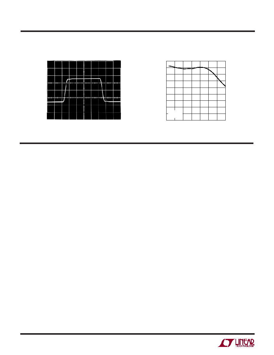
HORIZONTAL: 0.1ms/DIV, VERTICAL: 2V/DIV
VS = ±5V, fC = 10kHz, VIN = 1kHz ±3VP
SQUARE WAVE
1065 G16
Transient Response
Group Delay
PI FU CTIO S
U
UU
Power Supply Pins (Pins 6, 3, N Package)
The positive and negative supply pin should be bypassed
with a high quality 0.1
Fceramiccapacitor.Inapplications
where the clock pin (5) is externally swept to provide
several cutoff frequencies, the output DC offset variation
is minimized by connecting an additional 1
F solid tanta-
lum capacitor in parallel with the 0.1
F disc ceramic. This
technique was used to generate the graphs of the output
DC offset variation versus clock; they are illustrated in the
Typical Performance Characteristics section.
When the power supply voltage exceeds
±7V, and when
V – is applied before V+ (if V+ is allowed to go below
ground) connect a signal diode between the positive
supply pin and ground to prevent latch-up (see Typical
Applications).
Ground Pin (Pin 2, N Package)
The ground pin merges the internal analog and digital
ground paths. The potential of the ground pin is the
reference for the internal switched-capacitor resistors,
and the reference for the external clock. The positive input
of the internal op amp is also tied to the ground pin.
For dual supply operation, the ground pin should be
connected to a high quality AC and DC ground. A ground
plane, if possible, should be used. A poor ground will
degrade DC offset and it will increase clock feedthrough,
noise and distortion.
A small amount of AC current flows out of the ground pin
whether or not the internal oscillator is used. The fre-
quency of the ground current equals the frequency of the
clock. The average value of this current is approximately
55
A, 110A, 170A for ±2.5V, ±5V and ±7.5V supplies
respectively.
For single supply operation, the ground pin should be
preferably biased at half supply (see Typical Applications).
VOS Adjust Pin (Pin 8, N Package)
The VOS adjust pin can be used to trim any small amount
of output DC offset voltage or to introduce a desired output
DC level. The DC gain from the VOS adjust pin to the filter
output pin equals two.
Any DC voltage applied to this pin will reflect at the output
pin of the filter multiplied by two.
If the VOS adjust pin is not used, it should be shorted to the
ground pin. The DC bias current flowing into the VOS adjust
pin is typically 10pA.
The VOS adjust pin should always be connected to an AC
ground; AC signals applied to this pin will degrade the filter
response.
相关PDF资料 |
PDF描述 |
|---|---|
| VE-B0N-IY-F3 | CONVERTER MOD DC/DC 18.5V 50W |
| LTC1065ISW#TR | IC FILTER LP 5TH ORD LIN 16SOIC |
| VE-B0M-IY-F4 | CONVERTER MOD DC/DC 10V 50W |
| VE-B0M-IY-F1 | CONVERTER MOD DC/DC 10V 50W |
| LTC1065ISW#PBF | IC FILTR 5TH ORDR LOWPASS 16SOIC |
相关代理商/技术参数 |
参数描述 |
|---|---|
| LTC1065M | 制造商:LINER 制造商全称:Linear Technology 功能描述:DC Accurate, Clock-Tunable Linear Phase 5th Order Bessel Lowpass Filter |
| LTC1065MJ8 | 制造商:LINER 制造商全称:Linear Technology 功能描述:DC Accurate, Clock-Tunable Linear Phase 5th Order Bessel Lowpass Filter |
| LTC1066-1 | 制造商:LINER 制造商全称:Linear Technology 功能描述:14-Bit DC Accurate Clock-Tunable, 8th Order Elliptic or Linear Phase Lowpass Filter |
| LTC1066-1_09 | 制造商:LINER 制造商全称:Linear Technology 功能描述:14-Bit DC Accurate Clock-Tunable, 8th Order Elliptic or Linear Phase Lowpass Filter |
| LTC1066-1CS | 制造商:LINER 制造商全称:Linear Technology 功能描述:14-Bit DC Accurate Clock-Tunable, 8th Order Elliptic or Linear Phase Lowpass Filter |
发布紧急采购,3分钟左右您将得到回复。