- 您现在的位置:买卖IC网 > PDF目录11026 > LTC1065ISW#TRPBF (Linear Technology)IC FILTR 5TH ORDR LOWPASS 16SOIC PDF资料下载
参数资料
| 型号: | LTC1065ISW#TRPBF |
| 厂商: | Linear Technology |
| 文件页数: | 16/16页 |
| 文件大小: | 0K |
| 描述: | IC FILTR 5TH ORDR LOWPASS 16SOIC |
| 标准包装: | 1,000 |
| 滤波器类型: | 贝塞尔,低通开关电容器 |
| 频率 - 截止或中心: | 50kHz |
| 滤波器数: | 1 |
| 滤波器阶数: | 5th |
| 电源电压: | ±2.37 V ~ 8 V |
| 安装类型: | 表面贴装 |
| 封装/外壳: | 16-SOIC(0.295",7.50mm 宽) |
| 供应商设备封装: | 16-SOIC |
| 包装: | 带卷 (TR) |
9
LTC1065
1065fb
CLOCK FREQUENCY (MHz)
0.5
K
0.80
0.75
0.70
0.65
0.60
0.55
0.50
0.45
0.40
2.5
1065 F07
1.0
1.5
2.0
3.0
fCLK = K/RC
C = 10pF
TA = 70°C
VS = ±7.5V
VS = ±2.5V
VS = ±5V
CLOCK FREQUENCY (MHz)
0.5
K
0.80
0.75
0.70
0.65
0.60
0.55
0.50
0.45
0.40
2.5
1065 F06
1.0
1.5
2.0
3.0
fCLK = K/RC
C = 10pF
TA = 25°C
VS = ±7.5V
VS = ±2.5V
VS = ±5V
CLOCK FREQUENCY (kHz)
0
f CLK
CHANGE
NORMALIZED
TO
ITS
25
°C
VALUE
(%)
4
3
2
1
0
–1
–2
–3
–4
400
1065 F05
100
200
300
500
C = 200pF
TA = –40°C
TA = 85°C
VS = ±2.5V
VS = ±5V
VS = ±7.5V
VS = ±5V
VS = ±2.5V
U
S
A
O
PPLICATI
WU
U
I FOR ATIO
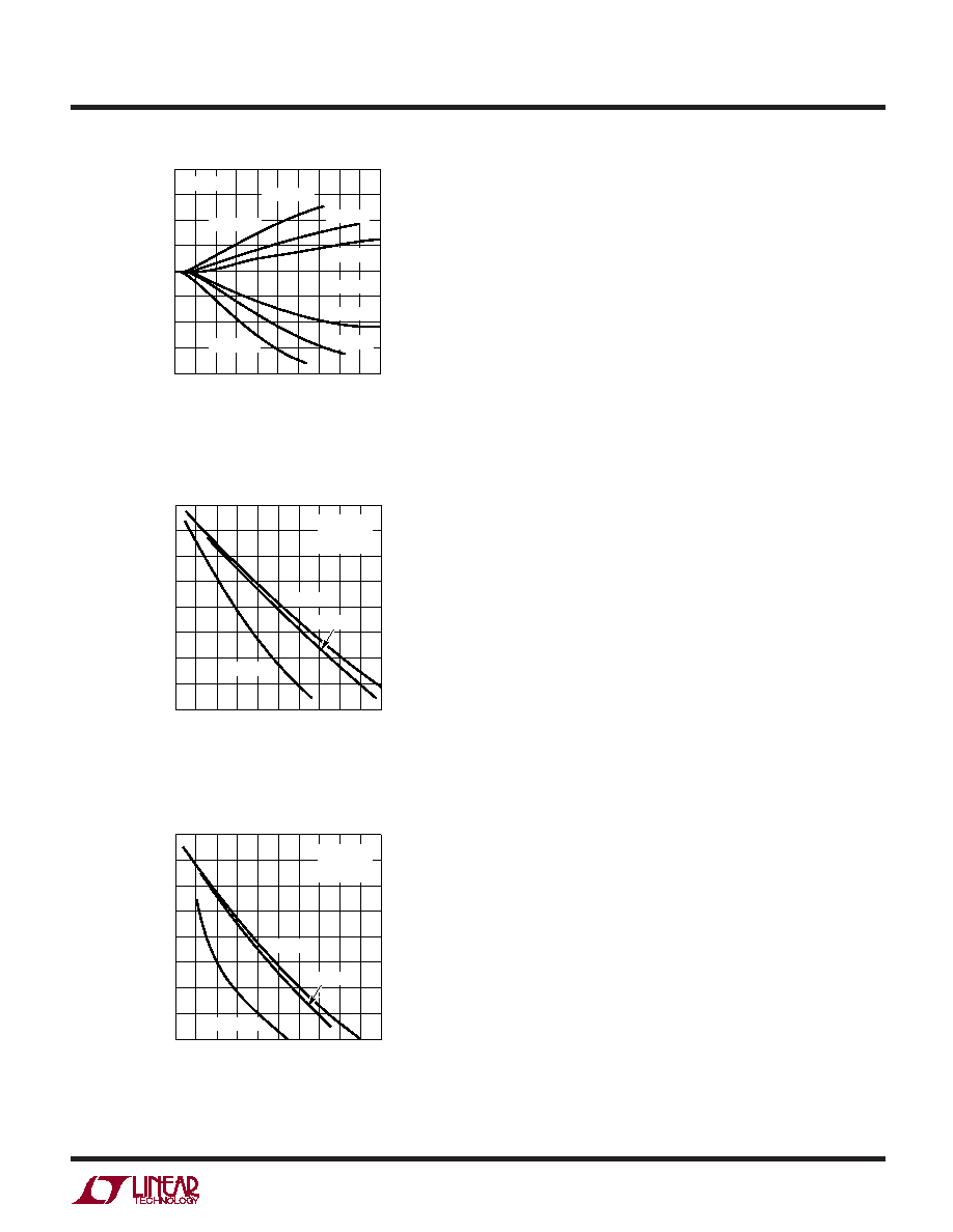
Figure 5. fCLK vs Temperature
Figure 6. fCLK vs K
Figure 7. fCLK vs K
A 4pF parasitic capacitance is assumed in parallel with the
external 10pF capacitor. A
±1% clock frequency variation
from device to device can be expected. The 2MHz clock
frequency designed above will typically drift to 1.74MHz at
70
°C (Figure 7).
The internal clock of the LTC1065 can be overridden by an
external clock provided that the external clock source can
drive the timing capacitor C, which is connected from the
clock input pin to ground.
Output Offset
The DC output offset of the LTC1065 is trimmed to
typically less than
±1mV. The trimming is done at VS =
±5V.ToobtainoptimumDCoffsetperformance,appropri-
ate PC layout techniques should be used and the filter IC
should be soldered to the PC board. A socket will degrade
the output DC offset by typically 1mV. The output DC offset
is sensitive to the coupling of the clock output pin 4 (N
package) to the negative power supply pin 3 (N package).
The negative supply pin should be well decoupled. When
the surface mount package is used, all NC pins should be
grounded. When the output DC voltage is measured with
a voltmeter, the filter output pin should be buffered. Long
test leads should be avoided.
With fixed power supplies, the output DC offset should not
change by more than
±100V over 10Hz to 1MHz clock
frequency variation. When the filter clock frequency is
fixed, the output DC offset will typically change by – 4mV
(2mV) when the power supply varies from
±5V to ±7.5V
(
±2.5V). See Typical Performance Characteristics.
Common Mode Rejection
The common mode rejection is defined as the change of
the output DC offset with respect to the DC change of the
input voltage applied to the filter.
CMR = 20log (
VOS OUT/VIN)(dB)
Table 3 illustrates the common mode rejection for three
power supplies and three temperatures. The common
mode rejection improves if the output offset is adjusted to
approximately 0V. The output offset can be adjusted via
pin 8 (N package). See Typical Applications.
相关PDF资料 |
PDF描述 |
|---|---|
| VE-B0N-IY-F3 | CONVERTER MOD DC/DC 18.5V 50W |
| LTC1065ISW#TR | IC FILTER LP 5TH ORD LIN 16SOIC |
| VE-B0M-IY-F4 | CONVERTER MOD DC/DC 10V 50W |
| VE-B0M-IY-F1 | CONVERTER MOD DC/DC 10V 50W |
| LTC1065ISW#PBF | IC FILTR 5TH ORDR LOWPASS 16SOIC |
相关代理商/技术参数 |
参数描述 |
|---|---|
| LTC1065M | 制造商:LINER 制造商全称:Linear Technology 功能描述:DC Accurate, Clock-Tunable Linear Phase 5th Order Bessel Lowpass Filter |
| LTC1065MJ8 | 制造商:LINER 制造商全称:Linear Technology 功能描述:DC Accurate, Clock-Tunable Linear Phase 5th Order Bessel Lowpass Filter |
| LTC1066-1 | 制造商:LINER 制造商全称:Linear Technology 功能描述:14-Bit DC Accurate Clock-Tunable, 8th Order Elliptic or Linear Phase Lowpass Filter |
| LTC1066-1_09 | 制造商:LINER 制造商全称:Linear Technology 功能描述:14-Bit DC Accurate Clock-Tunable, 8th Order Elliptic or Linear Phase Lowpass Filter |
| LTC1066-1CS | 制造商:LINER 制造商全称:Linear Technology 功能描述:14-Bit DC Accurate Clock-Tunable, 8th Order Elliptic or Linear Phase Lowpass Filter |
发布紧急采购,3分钟左右您将得到回复。