- 您现在的位置:买卖IC网 > PDF目录10689 > LTC1098CN8#PBF (Linear Technology)IC A/D CONV 8BIT SRL IN/OUT 8DIP PDF资料下载
参数资料
| 型号: | LTC1098CN8#PBF |
| 厂商: | Linear Technology |
| 文件页数: | 15/32页 |
| 文件大小: | 0K |
| 描述: | IC A/D CONV 8BIT SRL IN/OUT 8DIP |
| 标准包装: | 50 |
| 位数: | 8 |
| 采样率(每秒): | 33k |
| 数据接口: | 串行 |
| 转换器数目: | 1 |
| 功率耗散(最大): | 780µW |
| 电压电源: | 单电源 |
| 工作温度: | 0°C ~ 70°C |
| 安装类型: | 通孔 |
| 封装/外壳: | 8-DIP(0.300",7.62mm) |
| 供应商设备封装: | 8-PDIP |
| 包装: | 管件 |
| 输入数目和类型: | 1 个差分,单极 |
| 产品目录页面: | 1345 (CN2011-ZH PDF) |
第1页第2页第3页第4页第5页第6页第7页第8页第9页第10页第11页第12页第13页第14页当前第15页第16页第17页第18页第19页第20页第21页第22页第23页第24页第25页第26页第27页第28页第29页第30页第31页第32页
LTC1096/LTC1096L
LTC1098/LTC1098L
22
10968fc
in and continues until the falling CLK edge after the MSBF
bit is received. On this falling edge, the S&H goes into hold
mode and the conversion begins.
Differential Inputs
With differential inputs, the ADC no longer converts just a
single voltage but rather the difference between two volt-
ages. In this case, the voltage on the selected “+” input
is still sampled and held and therefore may be rapidly
time varying just as in single-ended mode. However, the
voltage on the selected “–” input must remain constant
and be free of noise and ripple throughout the conver-
sion time. Otherwise, the differencing operation may not
be performed accurately. The conversion time is 8 CLK
cycles. Therefore, a change in the “–” input voltage during
this interval can cause conversion errors. For a sinusoidal
voltage on the “–” input this error would be:
VERROR (MAX) = VPEAK 2 π f(“–”) 8/fCLK
Where f(“–”) is the frequency of the “–” input voltage,
VPEAK is its peak amplitude and fCLK is the frequency of
the CLK. In most cases VERROR will not be signicant. For
a 60Hz signal on the “–” input to generate a 1/4LSB error
(5mV) with the converter running at CLK = 500kHz, its
peak value would have to be 750mV.
ANALOG INPUTS
Because of the capacitive redistribution A/D conversion
techniques used, the analog inputs of the LTC1096(L)/
LTC1098(L )have capacitive switching input current spikes.
These current spikes settle quickly and do not cause a
problem. However, if large source resistances are used
or if slow settling op amps drive the inputs, care must be
taken to ensure that the transients caused by the current
spikes settle completely before the conversion begins.
“+” Input Settling
The input capacitor of the LTC1096(L) is switched onto
“+” input during the wake-up time (see Figure 1) and
samples the input signal within that time. However, the
input capacitor of the LTC1098(L) is switched onto “+”
input during the sample phase (tSMPL, see Figure 7). The
sample phase is 1.5 CLK cycles before conversion starts.
The voltage on the “+” input must settle completely within
tWAKEUP or tSMPL for the LTC1096(L) or the LTC1098(L)
respectively. Minimizing RSOURCE+ and C1 will improve the
input settling time. If a large “+” input source resistance
must be used, the sample time can be increased by using
a slower CLK frequency.
“–” Input Settling
At the end of the tWAKEUP or tSMPL, the input capacitor
switches to the “–” input and conversion starts (see
Figures 1 and 7). During the conversion the “+” input
voltage is effectively “held” by the sample-and-hold and
will not affect the conversion result. However, it is criti-
cal that the “–” input voltage settles completely during
the rst CLK cycle of the conversion time and be free of
noise. Minimizing RSOURCE– and C2 will improve settling
time. If a large “–” input source resistance must be used,
the time allowed for settling can be extended by using a
slower CLK frequency.
Input Op Amps
When driving the analog inputs with an op amp it is im-
portant that the op amp settle within the allowed time (see
Figure 7). Again, the “+” and “–” input sampling times can
be extended as described above to accommodate slower
op amps. Most op amps, including the LT1006 and LT1413
single supply op amps, can be made to settle well even
with the minimum settling windows of 3μs (“+” input)
which occur at the maximum clock rate of 500kHz.
Source Resistance
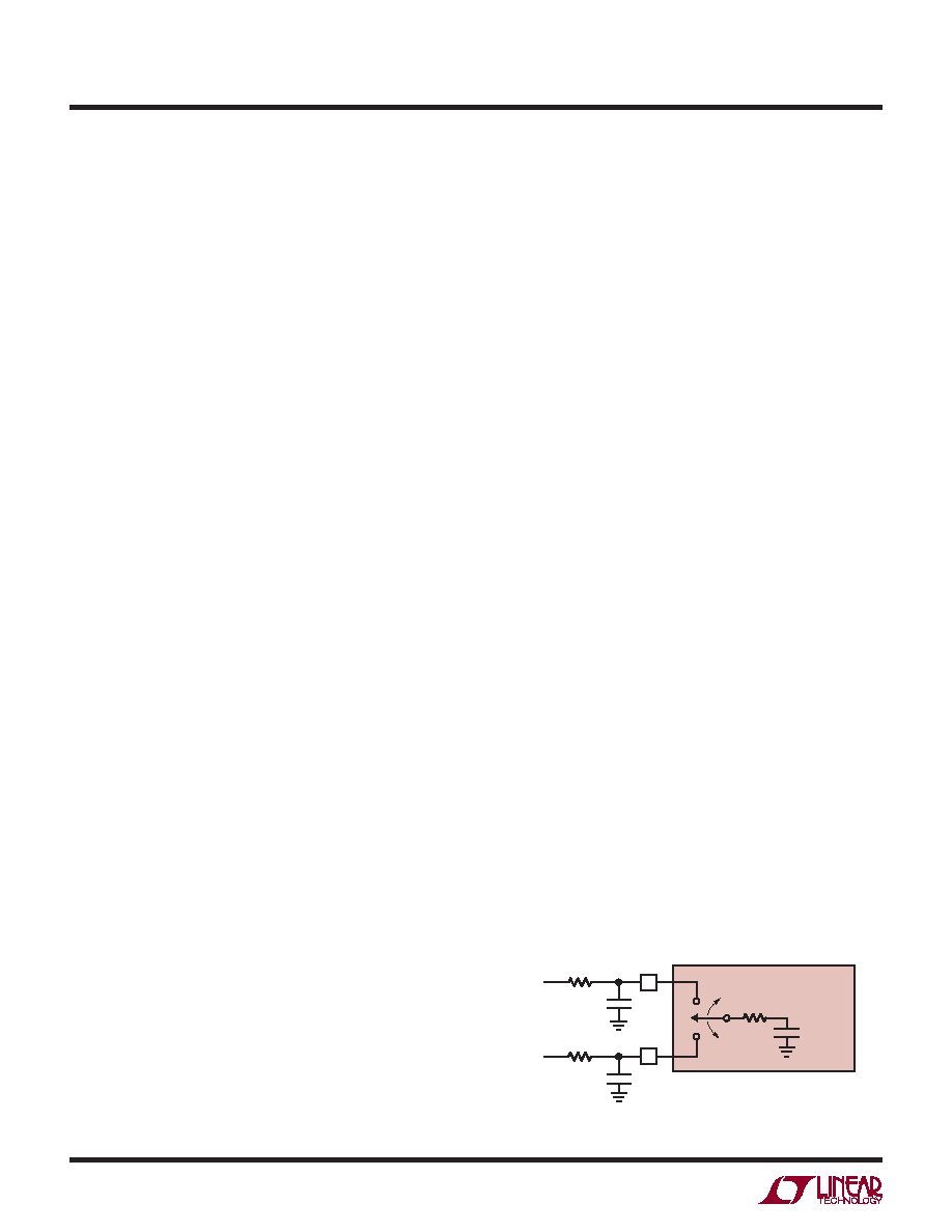
The analog inputs of the LTC1096/LTC1098 look like a 25pF
capacitor (CIN) in series with a 500Ω resistor (RON) as
shown in Figure 8. CIN gets switched between the selected
“+” and “–” inputs once during each conversion cycle.
Figure 8. Analog Input Equivalent Circuit
RON = 500Ω
CIN = 25pF
LTC1096
LTC1098
“+”
INPUT
RSOURCE
+
VIN +
C1
“–”
INPUT
RSOURCE
–
VIN –
C2
10968 F08
APPLICATIONS INFORMATION
相关PDF资料 |
PDF描述 |
|---|---|
| LTC1443CS#TRPBF | IC COMP W/REF LOWPWR QUAD 16SOIC |
| AD7920AKSZ-500RL7 | IC ADC 12BIT SRL 250KSPS SC70-6 |
| LTC1443CS#TR | IC COMP QUAD LP 1.182VREF 16SOIC |
| AD8611ARZ-REEL | IC COMP SGL 4NS ULTRFAST 8SOIC |
| AD9280ARSZ | IC ADC CMOS 8BIT 32MSPS 28-SSOP |
相关代理商/技术参数 |
参数描述 |
|---|---|
| LTC1098CN8-TR | 制造商:LINER 制造商全称:Linear Technology 功能描述:Micropower Sampling 8-Bit Serial I/O A/D Converters |
| LTC1098CN8-TRPBF | 制造商:LINER 制造商全称:Linear Technology 功能描述:Micropower Sampling 8-Bit Serial I/O A/D Converters |
| LTC1098CS8 | 功能描述:IC A/D CONV 8BIT SRL IN/OUT8SOIC RoHS:否 类别:集成电路 (IC) >> 数据采集 - 模数转换器 系列:- 标准包装:2,500 系列:- 位数:16 采样率(每秒):15 数据接口:MICROWIRE?,串行,SPI? 转换器数目:1 功率耗散(最大):480µW 电压电源:单电源 工作温度:-40°C ~ 85°C 安装类型:表面贴装 封装/外壳:38-WFQFN 裸露焊盘 供应商设备封装:38-QFN(5x7) 包装:带卷 (TR) 输入数目和类型:16 个单端,双极;8 个差分,双极 配用:DC1011A-C-ND - BOARD DELTA SIGMA ADC LTC2494 |
| LTC1098CS8#PBF | 功能描述:IC A/D CONV 8BIT SRL IN/OUT8SOIC RoHS:是 类别:集成电路 (IC) >> 数据采集 - 模数转换器 系列:- 其它有关文件:TSA1204 View All Specifications 标准包装:1 系列:- 位数:12 采样率(每秒):20M 数据接口:并联 转换器数目:2 功率耗散(最大):155mW 电压电源:模拟和数字 工作温度:-40°C ~ 85°C 安装类型:表面贴装 封装/外壳:48-TQFP 供应商设备封装:48-TQFP(7x7) 包装:Digi-Reel® 输入数目和类型:4 个单端,单极;2 个差分,单极 产品目录页面:1156 (CN2011-ZH PDF) 其它名称:497-5435-6 |
| LTC1098CS8#TR | 功能描述:IC ADC 8BIT SERIAL I/O 5V 8SOIC RoHS:否 类别:集成电路 (IC) >> 数据采集 - 模数转换器 系列:- 标准包装:2,500 系列:- 位数:16 采样率(每秒):15 数据接口:MICROWIRE?,串行,SPI? 转换器数目:1 功率耗散(最大):480µW 电压电源:单电源 工作温度:-40°C ~ 85°C 安装类型:表面贴装 封装/外壳:38-WFQFN 裸露焊盘 供应商设备封装:38-QFN(5x7) 包装:带卷 (TR) 输入数目和类型:16 个单端,双极;8 个差分,双极 配用:DC1011A-C-ND - BOARD DELTA SIGMA ADC LTC2494 |
发布紧急采购,3分钟左右您将得到回复。