- 您现在的位置:买卖IC网 > PDF目录377734 > LTC1159 (Linear Technology Corporation) RADIATION HARDENED HIGH EFFICIENCY, 5 AMP SWITCHING REGULATORS PDF资料下载
参数资料
| 型号: | LTC1159 |
| 厂商: | Linear Technology Corporation |
| 元件分类: | 基准电压源/电流源 |
| 英文描述: | RADIATION HARDENED HIGH EFFICIENCY, 5 AMP SWITCHING REGULATORS |
| 中文描述: | 抗辐射高效,5安培开关稳压器 |
| 文件页数: | 10/20页 |
| 文件大小: | 400K |
| 代理商: | LTC1159 |
10
LTC1159/LTC1159-3.3/LTC1159-5
APPLICATIU
W
U
U
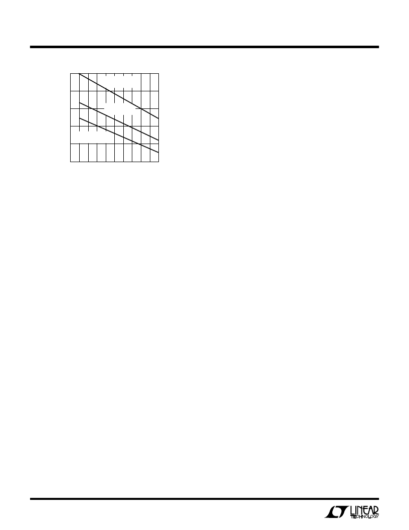
Figure 4. Minimum Suggested C
OUT
(V
IN
– V
OUT
) VOLTAGE (V)
0
C
O
μ
F600
800
1000
4
LTC1159 TPC04
400
200
0
1
2
3
5
L = 50
μ
H
R
SENSE
= 0.02
L = 25
μ
H
R
SENSE
= 0.02
L = 50
μ
H
R
SENSE
= 0.05
pronounced with low values of R
SENSE
and can be
improved by operating at higher frequencies with lower
values of L. The output remains in regulation at all times.
Load Transient Response
Switching regulators take several cycles to respond to a
step in DC (resistive) load current. When a load step
occurs, V
OUT
shifts by an amount equal to
I
LOAD
×
ESR,
where ESR is the effective series resistance of C
OUT
.
I
LOAD
also begins to charge or discharge C
OUT
until the
regulator loop adapts to the current change and returns
V
OUT
to its steady state value. During this recovery time
V
OUT
can be monitored for overshoot or ringing which
would indicate a stability problem. The I
TH
external
components shown in the Figure 1 circuit will provide
adequate compensation for most applications.
A second, more severe transient is caused by switching in
loads with large (>1
μ
F) supply bypass capacitors. The
discharged bypass capacitors are effectively put in parallel
with C
OUT
, causing a rapid drop in V
OUT
. No regulator can
deliver enough current to prevent this problem if the load
switch resistance is low and it is driven quickly. The only
solution is to limit the rise time of the switch drive so that
the load rise time is limited to approximately 25
×
C
LOAD
.
Thus a 10
μ
F capacitor would require a 250
μ
s rise time,
limiting the charging current to about 200mA.
Line Transient Response
The LTC1159 has better than 60dB line rejection and is
generally impervious to large positive or negative line
voltage transients. However, one rarely occurring condi-
tion can cause the output voltage to overshoot if the proper
precautions are not observed. This condition is a negative
V
IN
transition of several volts followed within 100
μ
s by a
positive transition of greater than 0.5V/
μ
s slew rate.
The reason this condition rarely occurs is because it takes
tens of amps to slew the regulator input capacitor at this
rate! The solution is to add a diode between the cap and V
IN
pins of the LTC1159 as shown in several of the typical
application circuits. If you think your system could have
this problem, add the diode. Note that in surface mount
applications it can be combined with the P-gate diode by
using a low cost common cathode dual diode.
EXTV
CC
Pin Connection
The LTC1159 contains an internal PNP switch connected
between the EXTV
CC
and V
CC
pins. The switch closes and
supplies the V
CC
power whenever the EXTV
CC
pin is higher
in voltage than the 4.5V internal regulator. This allows the
MOSFET driver and control power to be derived from the
output during normal operation and from the internal
regulator when the output is out of regulation (start-up,
short circuit).
Significant efficiency gains can be realized by powering V
CC
from the output, since the V
IN
current resulting from the
driver and control currents will be scaled by a factor of
(Duty Cycle)/(Efficiency). For 5V regulators this simply
means connecting the EXTV
CC
pin directly to V
OUT
. How-
ever, for 3.3V and other low voltage regulators, additional
circuitry is required to derive V
CC
power from the output.
The following list summarizes the four possible connec-
tions for EXTV
CC
:
1. EXTV
CC
Left Open. This will cause V
CC
to be powered
only from the internal 4.5V regulator resulting in re-
duced MOSFET gate drive levels and an efficiency pen-
alty of up to 10% at high input voltages.
相关PDF资料 |
PDF描述 |
|---|---|
| LTC1164-5 | Low Power 8th Order Pin Selectable Butterworth or Bessel Lowpass Filter |
| LTC1164-5C | Low Power 8th Order Pin Selectable Butterworth or Bessel Lowpass Filter |
| LTC1164-5CJ | Octal Bus Transceivers With 3-State Outputs 20-PDIP 0 to 70 |
| LTC1164-5CN | Low Power 8th Order Pin Selectable Butterworth or Bessel Lowpass Filter |
| LTC1164-5CS | Low Power 8th Order Pin Selectable Butterworth or Bessel Lowpass Filter |
相关代理商/技术参数 |
参数描述 |
|---|---|
| LTC1159_01 | 制造商:LINER 制造商全称:Linear Technology 功能描述:High Efficiency Synchronous Step-Down Switching Regulators |
| LTC1159-3.3 | 制造商:LINER 制造商全称:Linear Technology 功能描述:High Efficiency Synchronous Step-Down Switching Regulators |
| LTC1159-5 | 制造商:LINER 制造商全称:Linear Technology 功能描述:High Efficiency Synchronous Step-Down Switching Regulators |
| LTC1159CG | 功能描述:IC REG CTRLR BUCK PWM CM 20-SSOP RoHS:否 类别:集成电路 (IC) >> PMIC - 稳压器 - DC DC 切换控制器 系列:- 标准包装:4,500 系列:PowerWise® PWM 型:控制器 输出数:1 频率 - 最大:1MHz 占空比:95% 电源电压:2.8 V ~ 5.5 V 降压:是 升压:无 回扫:无 反相:无 倍增器:无 除法器:无 Cuk:无 隔离:无 工作温度:-40°C ~ 125°C 封装/外壳:6-WDFN 裸露焊盘 包装:带卷 (TR) 配用:LM1771EVAL-ND - BOARD EVALUATION LM1771 其它名称:LM1771SSDX |
| LTC1159CG#PBF | 功能描述:IC REG CTRLR BUCK PWM CM 20-SSOP RoHS:是 类别:集成电路 (IC) >> PMIC - 稳压器 - DC DC 切换控制器 系列:- 标准包装:4,500 系列:PowerWise® PWM 型:控制器 输出数:1 频率 - 最大:1MHz 占空比:95% 电源电压:2.8 V ~ 5.5 V 降压:是 升压:无 回扫:无 反相:无 倍增器:无 除法器:无 Cuk:无 隔离:无 工作温度:-40°C ~ 125°C 封装/外壳:6-WDFN 裸露焊盘 包装:带卷 (TR) 配用:LM1771EVAL-ND - BOARD EVALUATION LM1771 其它名称:LM1771SSDX |
发布紧急采购,3分钟左右您将得到回复。