- 您现在的位置:买卖IC网 > PDF目录377734 > LTC1159 (Linear Technology Corporation) RADIATION HARDENED HIGH EFFICIENCY, 5 AMP SWITCHING REGULATORS PDF资料下载
参数资料
| 型号: | LTC1159 |
| 厂商: | Linear Technology Corporation |
| 元件分类: | 基准电压源/电流源 |
| 英文描述: | RADIATION HARDENED HIGH EFFICIENCY, 5 AMP SWITCHING REGULATORS |
| 中文描述: | 抗辐射高效,5安培开关稳压器 |
| 文件页数: | 6/20页 |
| 文件大小: | 400K |
| 代理商: | LTC1159 |
6
LTC1159/LTC1159-3.3/LTC1159-5
When the voltage on C
T
has discharged past V
TH1
, com-
parator T trips, setting the flip-flop. This causes the N-gate
output to go low (turning off the N-channel MOSFET) and
the P-gate output to also go low (turning the P-channel
MOSFET back on). The cycle then repeats. As
the load
current increases, the output voltage decreases slightly.
This causes the output of the gain stage to increase the
current comparator threshold, thus tracking the load
current.
The sequence of events for Burst Mode operation is very
similar to continuous operation with the cycle interrupted
by the voltage comparator. When the output voltage is at or
above the desired regulated value, the P-channel MOSFET
is held off by comparator V and the timing capacitor
continues to discharge below V
TH1
. When the timing
capacitor discharges past V
TH2
, voltage comparator S
trips, causing the internal SLEEP line to go low and the
N-channel MOSFET to turn off.
The circuit now enters sleep mode with both power
MOSFETs turned off. In sleep mode, much of the cir-
cuitry is turned off, dropping the supply current from
several milliamps (with the MOSFETs switching) to
300
μ
A. When the output capacitor has discharged by
the amount of hysteresis in comparator V, the P-channel
MOSFET is again turned on and this process repeats. To
avoid the operation of the current loop interfering with
Burst Mode operation, a built-in offset is incorporated in
the gain stage.
To prevent both the external MOSFETs from being turned
on at the same time, feedback is incorporated to sense the
state of the driver output pins. Before the N-gate output can
go high, the P-drive output must also be high. Likewise, the
P-drive output is prevented from going low when the N-
gate output is high.
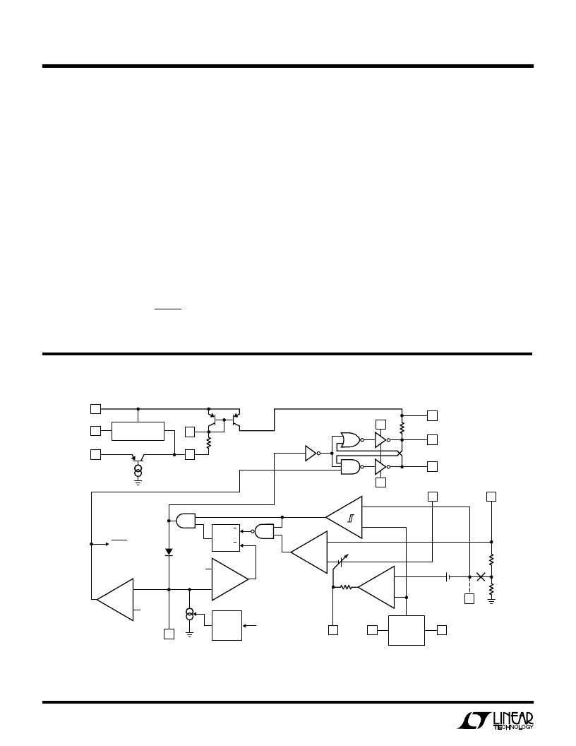
OPERATIOU
(Refer to Functional Diagram)
Internal divider broken at V
FB
for adjustable versions.
FU
W
–
+
N-GATE
P-DRIVE
V
CC
550k
P-GATE
P-GND
550k
CAP
LOW DROP SWITCH
V
CC
EXTV
CC
SHDN2
V
IN
–
+
–
+
SENSE
+
V
R
S
Q
V
TH1
–
+
25mV TO 150mV
13k
G
REFERENCE
1.25V
S-GND
I
TH
C
V
OS
SENSE
–
LTC1159 FD
SHDN1
–
+
T
V
TH2
S
SLEEP
C
T
V
FB
OFF-TIME
CONTROL
SENSE
–
LOW DROPOUT
4.5V REGULATOR
100k
相关PDF资料 |
PDF描述 |
|---|---|
| LTC1164-5 | Low Power 8th Order Pin Selectable Butterworth or Bessel Lowpass Filter |
| LTC1164-5C | Low Power 8th Order Pin Selectable Butterworth or Bessel Lowpass Filter |
| LTC1164-5CJ | Octal Bus Transceivers With 3-State Outputs 20-PDIP 0 to 70 |
| LTC1164-5CN | Low Power 8th Order Pin Selectable Butterworth or Bessel Lowpass Filter |
| LTC1164-5CS | Low Power 8th Order Pin Selectable Butterworth or Bessel Lowpass Filter |
相关代理商/技术参数 |
参数描述 |
|---|---|
| LTC1159_01 | 制造商:LINER 制造商全称:Linear Technology 功能描述:High Efficiency Synchronous Step-Down Switching Regulators |
| LTC1159-3.3 | 制造商:LINER 制造商全称:Linear Technology 功能描述:High Efficiency Synchronous Step-Down Switching Regulators |
| LTC1159-5 | 制造商:LINER 制造商全称:Linear Technology 功能描述:High Efficiency Synchronous Step-Down Switching Regulators |
| LTC1159CG | 功能描述:IC REG CTRLR BUCK PWM CM 20-SSOP RoHS:否 类别:集成电路 (IC) >> PMIC - 稳压器 - DC DC 切换控制器 系列:- 标准包装:4,500 系列:PowerWise® PWM 型:控制器 输出数:1 频率 - 最大:1MHz 占空比:95% 电源电压:2.8 V ~ 5.5 V 降压:是 升压:无 回扫:无 反相:无 倍增器:无 除法器:无 Cuk:无 隔离:无 工作温度:-40°C ~ 125°C 封装/外壳:6-WDFN 裸露焊盘 包装:带卷 (TR) 配用:LM1771EVAL-ND - BOARD EVALUATION LM1771 其它名称:LM1771SSDX |
| LTC1159CG#PBF | 功能描述:IC REG CTRLR BUCK PWM CM 20-SSOP RoHS:是 类别:集成电路 (IC) >> PMIC - 稳压器 - DC DC 切换控制器 系列:- 标准包装:4,500 系列:PowerWise® PWM 型:控制器 输出数:1 频率 - 最大:1MHz 占空比:95% 电源电压:2.8 V ~ 5.5 V 降压:是 升压:无 回扫:无 反相:无 倍增器:无 除法器:无 Cuk:无 隔离:无 工作温度:-40°C ~ 125°C 封装/外壳:6-WDFN 裸露焊盘 包装:带卷 (TR) 配用:LM1771EVAL-ND - BOARD EVALUATION LM1771 其它名称:LM1771SSDX |
发布紧急采购,3分钟左右您将得到回复。