- 您现在的位置:买卖IC网 > PDF目录1826 > LTC1159CG-5#PBF (Linear Technology)IC REG CTRLR BUCK PWM CM 20-SSOP PDF资料下载
参数资料
| 型号: | LTC1159CG-5#PBF |
| 厂商: | Linear Technology |
| 文件页数: | 14/20页 |
| 文件大小: | 0K |
| 描述: | IC REG CTRLR BUCK PWM CM 20-SSOP |
| 标准包装: | 66 |
| PWM 型: | 电流模式 |
| 输出数: | 1 |
| 频率 - 最大: | 250kHz |
| 占空比: | 100% |
| 电源电压: | 4 V ~ 40 V |
| 降压: | 是 |
| 升压: | 无 |
| 回扫: | 无 |
| 反相: | 无 |
| 倍增器: | 无 |
| 除法器: | 无 |
| Cuk: | 无 |
| 隔离: | 无 |
| 工作温度: | 0°C ~ 70°C |
| 封装/外壳: | 20-SSOP(0.209",5.30mm 宽) |
| 包装: | 管件 |
�� �
�
�LTC1159�
�LTC1159-3.3/LTC1159-5�
�APPLICATIO� S� I� FOR� ATIO�
�)�
�)�
�V� OFFSET� =� V� OUT�
�certain types of inductors in high current (I� OUT� > 5A)�
�applications� when� they� are� lightly� loaded.�
�An� external� offset� is� put� in� series� with� the� SENSE� –� pin� to�
�subtract� from� the� built-in� 0.025V� offset.� An� example� of� this�
�technique� is� shown� in� Figure� 7.� Two� 100� ?� resistors� are�
�inserted� in� series� with� the� leads� from� the� sense� resistor.�
�With� the� addition� of� R3,� a� current� is� generated� through� R1�
�causing� an� offset� of:�
�R1�
�R1� +� R3�
�If� V� OFFSET� >� 0.025V,� the� minimum� threshold� will� be�
�cancelled� and� Burst� Mode� operation� is� prevented� from�
�occurring.� Since� V� OFFSET� is� constant,� the� maximum� load�
�current� is� also� decreased� by� the� same� offset.� Thus,� to� get�
�back� to� the� same� I� MAX� ,� the� value� of� the� sense� resistor� must�
�be� reduced:�
�R� SENSE� ≈� 75� m� ?�
�I� MAX�
�To� prevent� noise� spikes� from� erroneously� tripping� the�
�current� comparator,� a� 1000pF� capacitor� is� needed� across�
�the� SENSE� –� and� SENSE� +� pins.�
�L�
�1�
�R� SENSE�
�2�
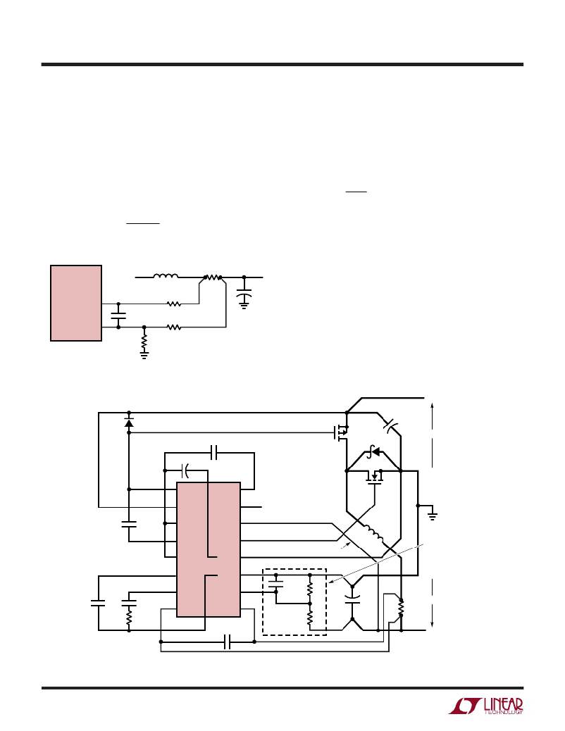
�Board� Layout� Checklist�
�LTC1159�
�SENSE� +�
�SENSE� –�
�9�
�8�
�1000pF�
�R2�
�100� ?�
�R1�
�100� ?�
�3�
�LTC1159� ?� F07�
�4�
�+�
�C� OUT�
�When� laying� out� the� printed� circuit� board,� the� following�
�checklist� should� be� used� to� ensure� proper� operation� of� the�
�LTC1159.� These� items� are� also� illustrated� graphically� in�
�the� layout� diagram� of� Figure� 8.� Check� the� following� in� your�
�R3�
�Figure� 7.� Suppressing� Burst� Mode� Operation�
�layout:�
�BOLD� LINES� INDICATE� HIGH� CURRENT� PATHS�
�+�
�1N4148�
�0.15� μ� F�
�P-CHANNEL�
�D1�
�C� IN�
�V� IN�
�1� μ� F�
�N-CHANNEL�
�–�
�1�
�P-GATE�
�CAP�
�16�
�2�
�V� IN�
�SHDN2�
�15�
�SHUTDOWN�
�0.1� μ� F�
�3�
�V� CC�
�EXTV� CC�
�14�
�L�
�4�
�5�
�6�
�P-DRIVE�
�V� CC�
�C� T�
�N-GATE�
�PGND�
�SGND�
�13�
�12�
�11�
�5V� EXTV� CC�
�CONNECTION�
�OUTPUT� DIVIDER�
�REQUIRED� WITH�
�ADJUSTABLE�
�VERSION� ONLY�
�–�
�C� T�
�3300pF�
�1k�
�7�
�8�
�I� TH�
�SENSE� –�
�V� FB�
�(SHDN1)�
�SENSE� +�
�10�
�9�
�100pF�
�R1�
�R2�
�C� OUT�
�3�
�1� V� OUT�
�R� SENSE�
�2�
�1000pF�
�4�
�+�
�LTC1159� ?� F08�
�Figure� 8.� LTC1159� Layout� Diagram� (N� and� S� Packages)�
�14�
�相关PDF资料 |
PDF描述 |
|---|---|
| LTC1174CN8-3.3#PBF | IC REG BUCK INV 3.3V 1A 8DIP |
| LTC1235CSW#TRPBF | IC MPU SUPERVISRY CIRCUIT 16SOIC |
| LTC1261CS | IC REG SWITCHED CAP INV 14SOIC |
| LTC1262IS8 | IC DC/DC CONV FLASHMEM 12V 8SOIC |
| LTC1263IS8#TR | IC CONV DC/DC FLASHMEM 12V 8SOIC |
相关代理商/技术参数 |
参数描述 |
|---|---|
| LTC1159CN | 制造商:LINER 制造商全称:Linear Technology 功能描述:High Efficiency Synchronous Step-Down Switching Regulators |
| LTC1159CN-3.3 | 制造商:LINER 制造商全称:Linear Technology 功能描述:High Efficiency Synchronous Step-Down Switching Regulators |
| LTC1159CN-5 | 制造商:LINER 制造商全称:Linear Technology 功能描述:High Efficiency Synchronous Step-Down Switching Regulators |
| LTC1159CS | 功能描述:IC REG CTRLR BUCK PWM CM 16-SOIC RoHS:否 类别:集成电路 (IC) >> PMIC - 稳压器 - DC DC 切换控制器 系列:- 标准包装:4,500 系列:PowerWise® PWM 型:控制器 输出数:1 频率 - 最大:1MHz 占空比:95% 电源电压:2.8 V ~ 5.5 V 降压:是 升压:无 回扫:无 反相:无 倍增器:无 除法器:无 Cuk:无 隔离:无 工作温度:-40°C ~ 125°C 封装/外壳:6-WDFN 裸露焊盘 包装:带卷 (TR) 配用:LM1771EVAL-ND - BOARD EVALUATION LM1771 其它名称:LM1771SSDX |
| LTC1159CS#PBF | 功能描述:IC REG CTRLR BUCK PWM CM 16-SOIC RoHS:是 类别:集成电路 (IC) >> PMIC - 稳压器 - DC DC 切换控制器 系列:- 标准包装:2,000 系列:- PWM 型:电流模式 输出数:1 频率 - 最大:1MHz 占空比:50% 电源电压:9 V ~ 10 V 降压:无 升压:是 回扫:是 反相:无 倍增器:无 除法器:无 Cuk:无 隔离:无 工作温度:-40°C ~ 85°C 封装/外壳:8-TSSOP(0.173",4.40mm 宽) 包装:带卷 (TR) |
发布紧急采购,3分钟左右您将得到回复。