- 您现在的位置:买卖IC网 > PDF目录1826 > LTC1159CG-5#PBF (Linear Technology)IC REG CTRLR BUCK PWM CM 20-SSOP PDF资料下载
参数资料
| 型号: | LTC1159CG-5#PBF |
| 厂商: | Linear Technology |
| 文件页数: | 6/20页 |
| 文件大小: | 0K |
| 描述: | IC REG CTRLR BUCK PWM CM 20-SSOP |
| 标准包装: | 66 |
| PWM 型: | 电流模式 |
| 输出数: | 1 |
| 频率 - 最大: | 250kHz |
| 占空比: | 100% |
| 电源电压: | 4 V ~ 40 V |
| 降压: | 是 |
| 升压: | 无 |
| 回扫: | 无 |
| 反相: | 无 |
| 倍增器: | 无 |
| 除法器: | 无 |
| Cuk: | 无 |
| 隔离: | 无 |
| 工作温度: | 0°C ~ 70°C |
| 封装/外壳: | 20-SSOP(0.209",5.30mm 宽) |
| 包装: | 管件 |
�� �
�
�LTC1159�
�LTC1159-3.3/LTC1159-5�
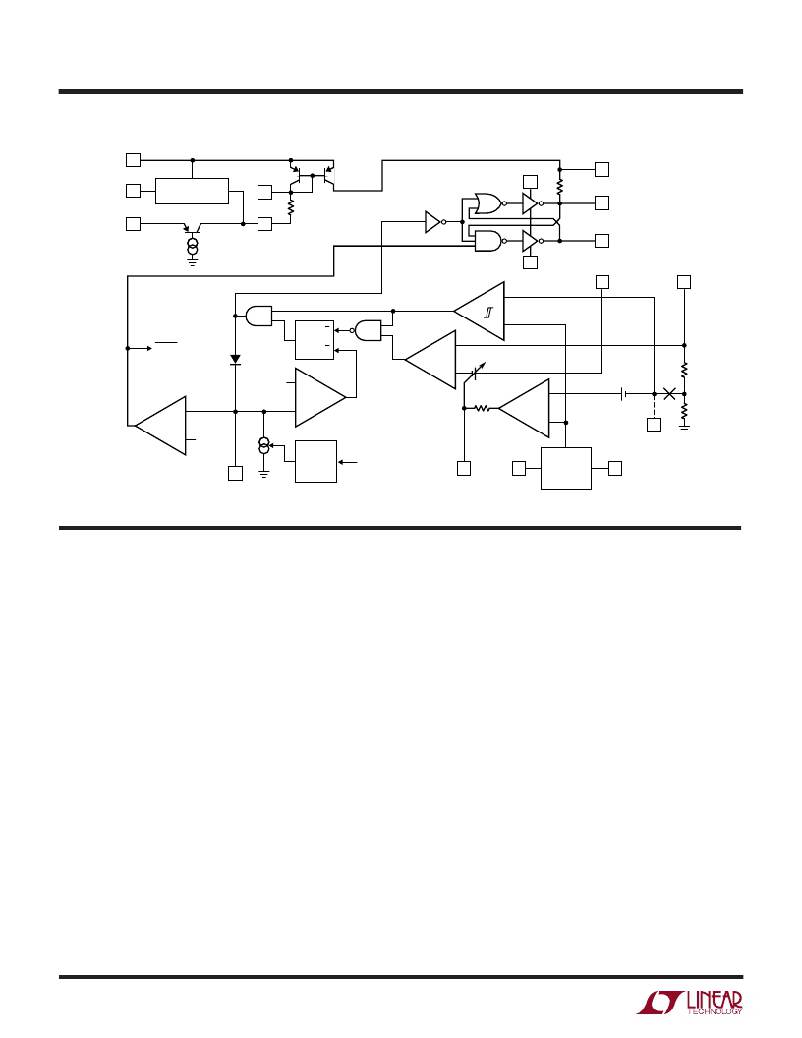
�FU� CTIO� AL� DIAGRA�
�Internal� divider� broken� at� V� FB� for� adjustable� versions.�
�V� IN�
�V� CC�
�P-GATE�
�SHDN2�
�EXTV� CC�
�LOW� DROPOUT�
�4.5V� REGULATOR�
�LOW� DROP� SWITCH�
�CAP�
�V� CC�
�550k�
�550k�
�P-DRIVE�
�N-GATE�
�R�
�V�
�PGND�
�SENSE� +�
�SENSE� –�
�SLEEP�
�Q�
�S�
�V� TH1�
�C�
�25mV� TO� 150mV�
�V� OS�
�+�
�T�
�13k�
�G�
�100k�
�S�
�–�
�V� TH2�
�1.25V�
�V� FB�
�LTC1159� ?� FD�
�OFF-TIME�
�CONTROL�
�SENSE� –�
�SGND�
�REFERENCE�
�SHDN1�
�C� T�
�I� TH�
�OPERATIO�
�(Refer� to� Functional� Diagram)�
�The� LTC1159� uses� a� current� mode,� constant� off-time�
�architecture� to� synchronously� switch� an� external� pair� of�
�complementary� power� MOSFETs.� Operating� frequency� is�
�set� by� an� external� capacitor� at� the� C� T� pin.�
�The� output� voltage� is� sensed� either� by� an� internal� voltage�
�divider� connected� to� the� SENSE� –� pin� (LTC1159-3.3� and�
�LTC1159-5)� or� an� external� divider� returned� to� the� V� FB� pin�
�(LTC1159).� A� voltage� comparator� V,� and� a� gain� block� G,�
�compare� the� divided� output� voltage� with� a� reference� volt-�
�age� of� 1.25V.� To� optimize� efficiency,� the� LTC1159� auto-�
�matically� switches� between� two� modes� of� operation,� burst�
�and� continuous.�
�A� low� dropout� 4.5V� regulator� provides� the� operating� volt-�
�age� V� CC� for� the� MOSFET� drivers� and� control� circuitry� during�
�start-up.� During� normal� operation,� the� LTC1159� family�
�powers� the� drivers� and� control� from� the� output� via� the�
�EXTV� CC� pin� to� improve� efficiency.� The� N-GATE� pin� is�
�referenced� to� ground� and� drives� the� N-channel� MOSFET�
�gate� directly.� The� P-channel� gate� drive� must� be� referenced�
�to� the� main� supply� input� V� IN� ,� which� is� accomplished� by�
�6�
�level-shifting� the� P-drive� signal� via� an� internal� 550k� resistor�
�and� external� capacitor.�
�During� the� switch� “ON”� cycle� in� continuous� mode,� current�
�comparator� C� monitors� the� voltage� between� the� SENSE� +�
�and� SENSE� –� pins� connected� across� an� external� shunt� in�
�series� with� the� inductor.� When� the� voltage� across� the� shunt�
�reaches� its� threshold� value,� the� P-gate� output� is� switched�
�to� V� IN� ,� turning� off� the� P-channel� MOSFET.� The� timing�
�capacitor� C� T� is� now� allowed� to� discharge� at� a� rate� deter-�
�mined� by� the� off-time� controller.� The� discharge� current� is�
�made� proportional� to� the� output� voltage� to� model� the�
�inductor� current,� which� decays� at� a� rate� which� is� also�
�proportional� to� the� output� voltage.� While� the� timing�
�capacitor� is� discharging,� the� N-gate� output� is� high,� turning�
�on� the� N-channel� MOSFET.�
�When� the� voltage� on� C� T� has� discharged� past� V� TH1� ,� compara-�
�tor� T� trips,� setting� the� flip-flop.� This� causes� the� N-gate� output�
�to� go� low� (turning� off� the� N-channel� MOSFET)� and� the� P-�
�gate� output� to� also� go� low� (turning� the� P-channel� MOSFET�
�back� on).� The� cycle� then� repeats.� As� the� load� current�
�相关PDF资料 |
PDF描述 |
|---|---|
| LTC1174CN8-3.3#PBF | IC REG BUCK INV 3.3V 1A 8DIP |
| LTC1235CSW#TRPBF | IC MPU SUPERVISRY CIRCUIT 16SOIC |
| LTC1261CS | IC REG SWITCHED CAP INV 14SOIC |
| LTC1262IS8 | IC DC/DC CONV FLASHMEM 12V 8SOIC |
| LTC1263IS8#TR | IC CONV DC/DC FLASHMEM 12V 8SOIC |
相关代理商/技术参数 |
参数描述 |
|---|---|
| LTC1159CN | 制造商:LINER 制造商全称:Linear Technology 功能描述:High Efficiency Synchronous Step-Down Switching Regulators |
| LTC1159CN-3.3 | 制造商:LINER 制造商全称:Linear Technology 功能描述:High Efficiency Synchronous Step-Down Switching Regulators |
| LTC1159CN-5 | 制造商:LINER 制造商全称:Linear Technology 功能描述:High Efficiency Synchronous Step-Down Switching Regulators |
| LTC1159CS | 功能描述:IC REG CTRLR BUCK PWM CM 16-SOIC RoHS:否 类别:集成电路 (IC) >> PMIC - 稳压器 - DC DC 切换控制器 系列:- 标准包装:4,500 系列:PowerWise® PWM 型:控制器 输出数:1 频率 - 最大:1MHz 占空比:95% 电源电压:2.8 V ~ 5.5 V 降压:是 升压:无 回扫:无 反相:无 倍增器:无 除法器:无 Cuk:无 隔离:无 工作温度:-40°C ~ 125°C 封装/外壳:6-WDFN 裸露焊盘 包装:带卷 (TR) 配用:LM1771EVAL-ND - BOARD EVALUATION LM1771 其它名称:LM1771SSDX |
| LTC1159CS#PBF | 功能描述:IC REG CTRLR BUCK PWM CM 16-SOIC RoHS:是 类别:集成电路 (IC) >> PMIC - 稳压器 - DC DC 切换控制器 系列:- 标准包装:2,000 系列:- PWM 型:电流模式 输出数:1 频率 - 最大:1MHz 占空比:50% 电源电压:9 V ~ 10 V 降压:无 升压:是 回扫:是 反相:无 倍增器:无 除法器:无 Cuk:无 隔离:无 工作温度:-40°C ~ 85°C 封装/外壳:8-TSSOP(0.173",4.40mm 宽) 包装:带卷 (TR) |
发布紧急采购,3分钟左右您将得到回复。