- 您现在的位置:买卖IC网 > PDF目录15253 > LTC1159IS-5#TRPBF (Linear Technology)IC REG CTRLR BUCK PWM CM 16-SOIC PDF资料下载
参数资料
| 型号: | LTC1159IS-5#TRPBF |
| 厂商: | Linear Technology |
| 文件页数: | 15/20页 |
| 文件大小: | 0K |
| 描述: | IC REG CTRLR BUCK PWM CM 16-SOIC |
| 标准包装: | 2,500 |
| PWM 型: | 电流模式 |
| 输出数: | 1 |
| 频率 - 最大: | 250kHz |
| 占空比: | 100% |
| 电源电压: | 4 V ~ 40 V |
| 降压: | 是 |
| 升压: | 无 |
| 回扫: | 无 |
| 反相: | 无 |
| 倍增器: | 无 |
| 除法器: | 无 |
| Cuk: | 无 |
| 隔离: | 无 |
| 工作温度: | -40°C ~ 85°C |
| 封装/外壳: | 16-SOIC(0.154",3.90mm 宽) |
| 包装: | 带卷 (TR) |
�� �
�
�LTC1159�
�LTC1159-3.3/LTC1159-5�
�APPLICATIO� S� I� FOR� ATIO�
�1)� Are� the� signal� and� power� grounds� segregated?� The�
�LTC1159� signal� ground� must� connect� separately� to� the�
�(–)� plate� of� C� OUT� .� The� other� ground� pin(s)� should� return� to�
�the� source� of� the� N-channel� MOSFET,� anode� of� the� Schot-�
�tky� diode� and� (–)� plate� of� C� IN� ,� which� should� have� as� short�
�lead� lengths� as� possible.�
�2)� Does� the� LTC1159� SENSE� –� pin� connect� to� a� point� close�
�to� R� SENSE� and� the� (+)� plate� of� C� OUT� ?� In� adjustable� applica-�
�tions,� the� resistive� divider� R1,� R2� must� be� connected�
�between� the� (+)� plate� of� C� OUT� and� signal� ground.�
�3)� Are� the� SENSE� –� and� SENSE� +� leads� routed� together�
�with� minimum� PC� trace� spacing?� The� differential�
�decoupling� capacitor� between� the� two� SENSE� pins� should�
�be� as� close� as� possible� to� the� LTC1159.� Up� to� 100� ?� may�
�be� placed� in� series� with� each� sense� lead� to� help� decouple�
�the� SENSE� pins.� However,� when� these� resistors� are� used,�
�the� capacitor� should� be� no� larger� than� 1000pF.�
�4)� Does� the� (+)� plate� of� C� IN� connect� to� the� source� of� the�
�P-channel� MOSFET� as� closely� as� possible?� An� additional�
�0.1� μ� F� ceramic� capacitor� between� V� IN� and� power� ground�
�may� be� required� in� some� applications.�
�7)� Is� the� SHDN1� pin� actively� pulled� to� ground� during�
�normal� operation?� SHDN1� is� a� high� impedance� pin� and�
�must� not� be� allowed� to� float.�
�Troubleshooting� Hints�
�Since� efficiency� is� critical� to� LTC1159� applications� it� is� very�
�important� to� verify� that� the� circuit� is� functioning� correctly�
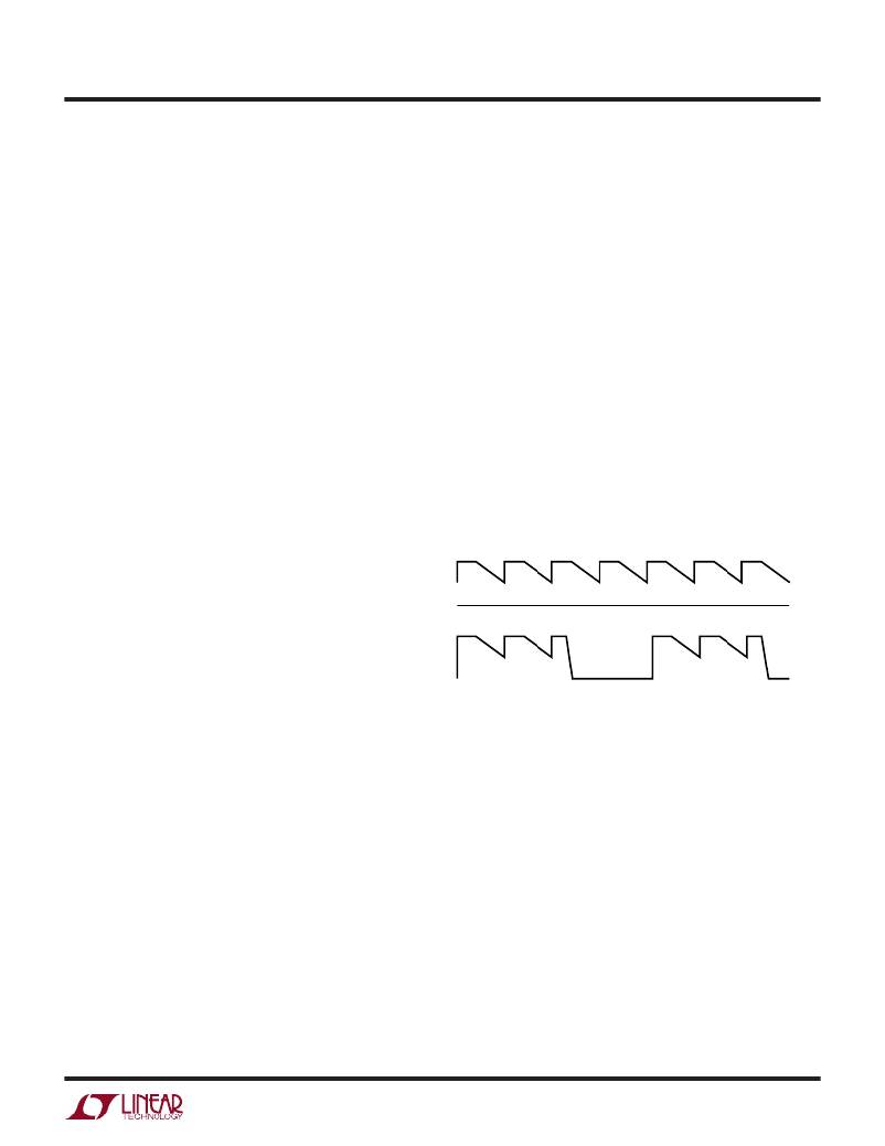
�in� both� continuous� and� Burst� Mode� operation.� The� wave-�
�form� to� monitor� is� the� voltage� on� the� C� T� pin� .�
�In� continuous� mode� (I� LOAD� >� I� BURST� )� the� voltage� should� be�
�a� sawtooth� with� a� 0.9V� P-P� swing.� This� voltage� should� never�
�dip� below� 2V� as� shown� in� Figure� 9a.� When� the� load� current�
�is� low� (I� LOAD� <� I� BURST� ),� Burst� Mode� operation� should� occur�
�with� the� C� T� waveform� periodically� falling� to� ground� as�
�shown� in� Figure� 9b.�
�If� the� C� T� pin� is� observed� falling� to� ground� at� high� output�
�currents,� it� indicates� poor� decoupling� or� improper� ground-�
�ing.� Refer� to� the� Board� Layout� Checklist.�
�3.3V�
�5)� Is� the� V� CC� decoupling� capacitor� connected� closely� be-�
�tween� the� V� CC� pins� of� the� LTC1159� and� power� ground?�
�This� capacitor� carries� the� MOSFET� driver� peak� currents.�
�6)� In� adjustable� versions,� the� feedback� pin� is� very� sensitive�
�to� pickup� from� the� switch� node.� Care� must� be� taken� to�
�isolate� V� FB� from� possible� capacitive� coupling� of� the� induc-�
�tor� switch� signal.�
�(a)� CONTINUOUS� MODE� OPERATION�
�(b)� Burst� Mode� OPERATION�
�Figure� 9.� C� T� Pin� 6� Waveforms�
�0V�
�3.3V�
�0V�
�LTC1159� ?� F09�
�15�
�相关PDF资料 |
PDF描述 |
|---|---|
| RGM15DRMN-S288 | CONN EDGECARD 30POS .156 EXTEND |
| 9250A-822-RC | CHOKE RF MOLDED 8.2UH IRON |
| RSM15DRMH-S288 | CONN EDGECARD 30POS .156 EXTEND |
| LTC1775IS#TRPBF | IC REG CTRLR BUCK PWM CM 16-SOIC |
| RMM15DRMH-S288 | CONN EDGECARD 30POS .156 EXTEND |
相关代理商/技术参数 |
参数描述 |
|---|---|
| LTC1160CN | 制造商:未知厂家 制造商全称:未知厂家 功能描述:Interface IC |
| LTC1160CS | 制造商:未知厂家 制造商全称:未知厂家 功能描述:Interface IC |
| LTC1160IN | 制造商:未知厂家 制造商全称:未知厂家 功能描述:Interface IC |
| LTC1160IS | 制造商:未知厂家 制造商全称:未知厂家 功能描述:Interface IC |
| LTC1162CN | 制造商:未知厂家 制造商全称:未知厂家 功能描述:Interface IC |
发布紧急采购,3分钟左右您将得到回复。