- 您现在的位置:买卖IC网 > PDF目录10351 > LTC1197IS8#TRPBF (Linear Technology)IC A/DCONV 10BIT W/SHTDWN 8-SOIC PDF资料下载
参数资料
| 型号: | LTC1197IS8#TRPBF |
| 厂商: | Linear Technology |
| 文件页数: | 5/28页 |
| 文件大小: | 0K |
| 描述: | IC A/DCONV 10BIT W/SHTDWN 8-SOIC |
| 标准包装: | 2,500 |
| 位数: | 10 |
| 采样率(每秒): | 500k |
| 数据接口: | MICROWIRE?,串行,SPI? |
| 转换器数目: | 1 |
| 功率耗散(最大): | 25mW |
| 电压电源: | 单电源 |
| 工作温度: | -40°C ~ 85°C |
| 安装类型: | 表面贴装 |
| 封装/外壳: | 8-SOIC(0.154",3.90mm 宽) |
| 供应商设备封装: | 8-SOIC |
| 包装: | 带卷 (TR) |
| 输入数目和类型: | 1 个差分,单极 |
第1页第2页第3页第4页当前第5页第6页第7页第8页第9页第10页第11页第12页第13页第14页第15页第16页第17页第18页第19页第20页第21页第22页第23页第24页第25页第26页第27页第28页
13
LTC1197/LTC1197L
LTC1199/LTC1199L
1197/99 F02
CLK
CS
tdDO
tsuCS
B0*
B1
B2
B3
B4
B5
B6
B7
B8
B9
NULL
BITS
Hi-Z
14
13
12
11
10
9
8
7
6
5
4
3
2
1
15
16
1
DOUT
DIN
HI-Z
START
DUMMY
DON’T CARE
ODD/
SIGN
SGL/
DIFF
*AFTER COMPLETING THE DATA TRANSFER, IF FURTHER CLOCKS ARE APPLIED WITH CS LOW,
THE ADC WILL OUTPUT ZEROS INDEFINITELY
ten
tCYC (16 CLKs)*
tCONV
(10.5 CLKs)
POWER
DOWN
tSMPL
(1.5 CLKs)
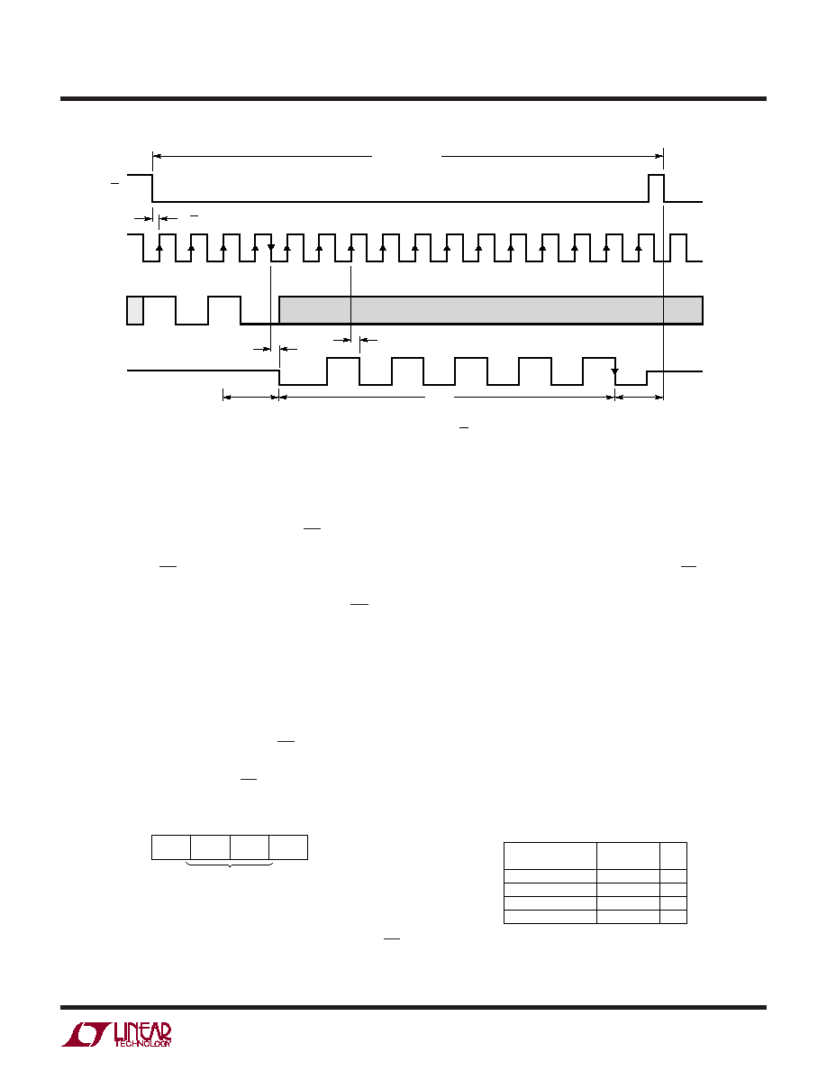
Figure 2. LTC1199/LTC1199L Operating Sequence
transfer and all leading zeros that precede this logical one
will be ignored. After the start bit is received the remaining
bits of the input word will be clocked in. Further inputs on
the DIN pin are then ignored until the next CS cycle.
Multiplexer (MUX) Address
The bits of the input word following the start bit assign the
MUX configuration for the requested conversion. For a
given channel selection, the converter will measure the
voltage between the two channels indicated by the “+” and
“–” signs in the selected row of the following table. In
single-ended mode, all input channels are measured with
respect to GND. Only the + inputs have sample-and-holds.
Signals applied at the – inputs must not change more than
the required accuracy during the conversion.
Multiplexer Channel Selection
MUX ADDRESS
SGL/DIFF
1
0
ODD/SIGN
0
1
0
1
CHANNEL #
0
+
–
1
+
–
+
GND
–
1197/99 AI02
The LTC1197/LTC1197L do not require a configuration
input word and have no DIN pin. A falling CS initiates data
transfer as shown in the LTC1197/LTC1197L operating
sequence. After CS falls, the second CLK pulse enables
DOUT. After two null bits, the A/D conversion result is output
on the DOUT line in MSB-first format. Bringing CS high
resets the LTC1197/LTC1197L for the next data exchange
and minimizes the supply current if CLK is continuously
running.
INPUT DATA WORD (LTC1199/LTC1199L ONLY)
The LTC1199 4-bit data word is clocked into the DIN input
on the rising edge of the clock after CS goes low and the
start bit has been recognized. Further inputs on the DIN pin
are then ignored until the next CS cycle. The input word is
defined as follows:
SGL/
DIFF
ODD/
SIGN
DUMMY
START
MUX
ADDRESS
1197/99 AI01
Start Bit
The first “logical one” clocked into the DIN input after CS
goes low is the start bit. The start bit initiates the data
APPLICATIO S I FOR ATIO
WU
UU
相关PDF资料 |
PDF描述 |
|---|---|
| VE-J3F-IW-B1 | CONVERTER MOD DC/DC 72V 100W |
| MS27497E22B21SLC | CONN HSG RCPT 21POS WALLMT SCKT |
| LTC1197IS8#TR | IC ADC 10BIT 500KHZ SHTDWN 8SOIC |
| VE-J3D-IW-B1 | CONVERTER MOD DC/DC 85V 100W |
| VE-26V-MX-S | CONVERTER MOD DC/DC 5.8V 75W |
相关代理商/技术参数 |
参数描述 |
|---|---|
| LTC1197L | 制造商:LINER 制造商全称:Linear Technology 功能描述:10-Bit, 500ksps ADCs in MSOP with Auto Shutdown |
| LTC1197LC | 制造商:LINER 制造商全称:Linear Technology 功能描述:10-Bit, 500ksps ADCs in MSOP with Auto Shutdown |
| LTC1197LCMS8 | 功能描述:IC ADC 10BIT 250KHZ W/SD 8-MSOP RoHS:否 类别:集成电路 (IC) >> 数据采集 - 模数转换器 系列:- 标准包装:2,500 系列:- 位数:16 采样率(每秒):15 数据接口:MICROWIRE?,串行,SPI? 转换器数目:1 功率耗散(最大):480µW 电压电源:单电源 工作温度:-40°C ~ 85°C 安装类型:表面贴装 封装/外壳:38-WFQFN 裸露焊盘 供应商设备封装:38-QFN(5x7) 包装:带卷 (TR) 输入数目和类型:16 个单端,双极;8 个差分,双极 配用:DC1011A-C-ND - BOARD DELTA SIGMA ADC LTC2494 |
| LTC1197LCMS8#PBF | 功能描述:IC ADC 10BIT 250KHZ W/SD 8-MSOP RoHS:是 类别:集成电路 (IC) >> 数据采集 - 模数转换器 系列:- 标准包装:2,500 系列:- 位数:16 采样率(每秒):15 数据接口:MICROWIRE?,串行,SPI? 转换器数目:1 功率耗散(最大):480µW 电压电源:单电源 工作温度:-40°C ~ 85°C 安装类型:表面贴装 封装/外壳:38-WFQFN 裸露焊盘 供应商设备封装:38-QFN(5x7) 包装:带卷 (TR) 输入数目和类型:16 个单端,双极;8 个差分,双极 配用:DC1011A-C-ND - BOARD DELTA SIGMA ADC LTC2494 |
| LTC1197LCMS8#TR | 功能描述:IC ADC 10BIT 250KHZ W/SD 8-MSOP RoHS:否 类别:集成电路 (IC) >> 数据采集 - 模数转换器 系列:- 标准包装:2,500 系列:- 位数:16 采样率(每秒):15 数据接口:MICROWIRE?,串行,SPI? 转换器数目:1 功率耗散(最大):480µW 电压电源:单电源 工作温度:-40°C ~ 85°C 安装类型:表面贴装 封装/外壳:38-WFQFN 裸露焊盘 供应商设备封装:38-QFN(5x7) 包装:带卷 (TR) 输入数目和类型:16 个单端,双极;8 个差分,双极 配用:DC1011A-C-ND - BOARD DELTA SIGMA ADC LTC2494 |
发布紧急采购,3分钟左右您将得到回复。