- 您现在的位置:买卖IC网 > PDF目录2003 > LTC1198-1BCS8#PBF (Linear Technology)IC ADC 8BIT 750KHZ SAMPL 8-SOIC PDF资料下载
参数资料
| 型号: | LTC1198-1BCS8#PBF |
| 厂商: | Linear Technology |
| 文件页数: | 10/28页 |
| 文件大小: | 0K |
| 描述: | IC ADC 8BIT 750KHZ SAMPL 8-SOIC |
| 标准包装: | 100 |
| 位数: | 8 |
| 采样率(每秒): | 750k |
| 数据接口: | 串行 |
| 转换器数目: | 1 |
| 功率耗散(最大): | 50mW |
| 电压电源: | 单电源 |
| 工作温度: | 0°C ~ 70°C |
| 安装类型: | 表面贴装 |
| 封装/外壳: | 8-SOIC(0.154",3.90mm 宽) |
| 供应商设备封装: | 8-SOIC |
| 包装: | 管件 |
| 输入数目和类型: | 1 个单端,单极 |
第1页第2页第3页第4页第5页第6页第7页第8页第9页当前第10页第11页第12页第13页第14页第15页第16页第17页第18页第19页第20页第21页第22页第23页第24页第25页第26页第27页第28页
LTC1196/LTC1198
18
119698fb
APPLICATIONS INFORMATION
Mixed Supplies
It is possible to have a digital system running off a 5V supply
and communicate with the LTC1196/LTC1198 operating on
a 3V supply. Achieving this reduces the outputs of DOUT
from the ADCs to toggle the equivalent input of the digital
system. The CS, CLK and DIN inputs of the ADCs will take
5V signals from the digital system without causing any
problem (see the Digital Input Logic Threshold vs Supply
Voltage curve in the Typical Performance Characteristics
section). With the LTC1196 operating on a 3V supply, the
output of DOUT only goes between 0V and 3V. This signal
easily meets TTL levels (see Figure 6).
BOARD LAYOUT CONSIDERATIONS
Grounding and Bypassing
The LTC1196/LTC1198 are easy to use if some care is
taken. They should be used with an analog ground plane
and single-point grounding techniques. The GND pin
should be tied directly to the ground plane.
The VCC pin should be bypassed to the ground plane with a
1μF tantalum with leads as short as possible. If the power
supply is clean, the LTC1196/LTC1198 can also operate
with smaller 0.1μF surface mount or ceramic bypass ca-
pacitors. All analog inputs should be referenced directly to
the single-point ground. Digital inputs and outputs should
be shielded from and/or routed away from the reference
and analog circuitry.
SAMPLE-AND-HOLD
Both the LTC1196 and the LTC1198 provide a built-in
sample-and-hold (S&H) function to acquire the input
signal. The S&H acquires the input signal from “+” input
during tSMPL as shown in Figures 1 and 2. The S&H of the
LTC1198 can sample input signals in either single-ended
or differential mode (see Figure 7).
3V
4.7μF
MPU
(e.g., 8051)
5V
P1.4
P1.3
P1.2
1196/98 F06
DIFFERENTIAL INPUTS
COMMON MODE RANGE
0V TO 3V
3V
VCC
CLK
DOUT
VREF
LTC1196
–IN
GND
+IN
CS
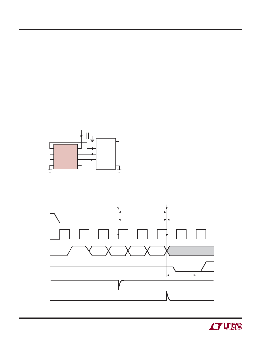
Figure 6. Interfacing a 3V Powered LTC1196 to a 5V System
CLK
DIN
DOUT
+ INPUT
– INPUT
D
L
O
H
E
L
P
M
A
S
+ INPUT MUST
SETTLE DURING
THIS TIME
tSMPL
tCONV
CS
START
SGL/DIFF
DUMMY
1ST BIT TEST:
– INPUT MUST SETTLE DURING THIS TIME
B7
1196/98 F07
ODD/SIGN
DUMMY
DON’T CARE
Figure 7. LTC1198 “+” and “–” Input Settling Windows
相关PDF资料 |
PDF描述 |
|---|---|
| LTC1257IS8#TRPBF | IC D/A CONV 12BIT VOLT OUT 8SOIC |
| LTC1276ACN#PBF | IC A/D CONV 12BIT SAMPLING 24DIP |
| LTC1278-4IN#PBF | IC A/DCONV SAMPLNG W/SHTDN 24DIP |
| LTC1279CG#TRPBF | IC A/DCONV SAMPLNG W/SHTDN24SSOP |
| LTC1282ACN#PBF | IC A/D CONV SAMPLING W/REF 24DIP |
相关代理商/技术参数 |
参数描述 |
|---|---|
| LTC1198-1BCS8-TRPBF | 制造商:LINER 制造商全称:Linear Technology 功能描述:8-Bit, SO-8, 1Msps ADCs with Auto-Shutdown Options |
| LTC1198-2AC | 制造商:LINER 制造商全称:Linear Technology 功能描述:8-Bit, SO-8, 1MSPS ADCs with Auto-Shutdown Options |
| LTC1198-2ACS8 | 功能描述:IC ADC 8BIT 750KHZ SAMPL 8-SOIC RoHS:否 类别:集成电路 (IC) >> 数据采集 - 模数转换器 系列:- 其它有关文件:TSA1204 View All Specifications 标准包装:1 系列:- 位数:12 采样率(每秒):20M 数据接口:并联 转换器数目:2 功率耗散(最大):155mW 电压电源:模拟和数字 工作温度:-40°C ~ 85°C 安装类型:表面贴装 封装/外壳:48-TQFP 供应商设备封装:48-TQFP(7x7) 包装:Digi-Reel® 输入数目和类型:4 个单端,单极;2 个差分,单极 产品目录页面:1156 (CN2011-ZH PDF) 其它名称:497-5435-6 |
| LTC1198-2ACS8#PBF | 功能描述:IC ADC 8BIT 750KHZ SAMPL 8-SOIC RoHS:是 类别:集成电路 (IC) >> 数据采集 - 模数转换器 系列:- 产品培训模块:Lead (SnPb) Finish for COTS Obsolescence Mitigation Program 标准包装:2,500 系列:- 位数:12 采样率(每秒):3M 数据接口:- 转换器数目:- 功率耗散(最大):- 电压电源:- 工作温度:- 安装类型:表面贴装 封装/外壳:SOT-23-6 供应商设备封装:SOT-23-6 包装:带卷 (TR) 输入数目和类型:- |
| LTC1198-2ACS8#TR | 功能描述:IC ADC 8BIT 750KHZ SHUTDWN 8SOIC RoHS:否 类别:集成电路 (IC) >> 数据采集 - 模数转换器 系列:- 标准包装:2,500 系列:- 位数:16 采样率(每秒):15 数据接口:MICROWIRE?,串行,SPI? 转换器数目:1 功率耗散(最大):480µW 电压电源:单电源 工作温度:-40°C ~ 85°C 安装类型:表面贴装 封装/外壳:38-WFQFN 裸露焊盘 供应商设备封装:38-QFN(5x7) 包装:带卷 (TR) 输入数目和类型:16 个单端,双极;8 个差分,双极 配用:DC1011A-C-ND - BOARD DELTA SIGMA ADC LTC2494 |
发布紧急采购,3分钟左右您将得到回复。