- 您现在的位置:买卖IC网 > PDF目录2003 > LTC1198-1BCS8#PBF (Linear Technology)IC ADC 8BIT 750KHZ SAMPL 8-SOIC PDF资料下载
参数资料
| 型号: | LTC1198-1BCS8#PBF |
| 厂商: | Linear Technology |
| 文件页数: | 17/28页 |
| 文件大小: | 0K |
| 描述: | IC ADC 8BIT 750KHZ SAMPL 8-SOIC |
| 标准包装: | 100 |
| 位数: | 8 |
| 采样率(每秒): | 750k |
| 数据接口: | 串行 |
| 转换器数目: | 1 |
| 功率耗散(最大): | 50mW |
| 电压电源: | 单电源 |
| 工作温度: | 0°C ~ 70°C |
| 安装类型: | 表面贴装 |
| 封装/外壳: | 8-SOIC(0.154",3.90mm 宽) |
| 供应商设备封装: | 8-SOIC |
| 包装: | 管件 |
| 输入数目和类型: | 1 个单端,单极 |
第1页第2页第3页第4页第5页第6页第7页第8页第9页第10页第11页第12页第13页第14页第15页第16页当前第17页第18页第19页第20页第21页第22页第23页第24页第25页第26页第27页第28页
LTC1196/LTC1198
24
119698fb
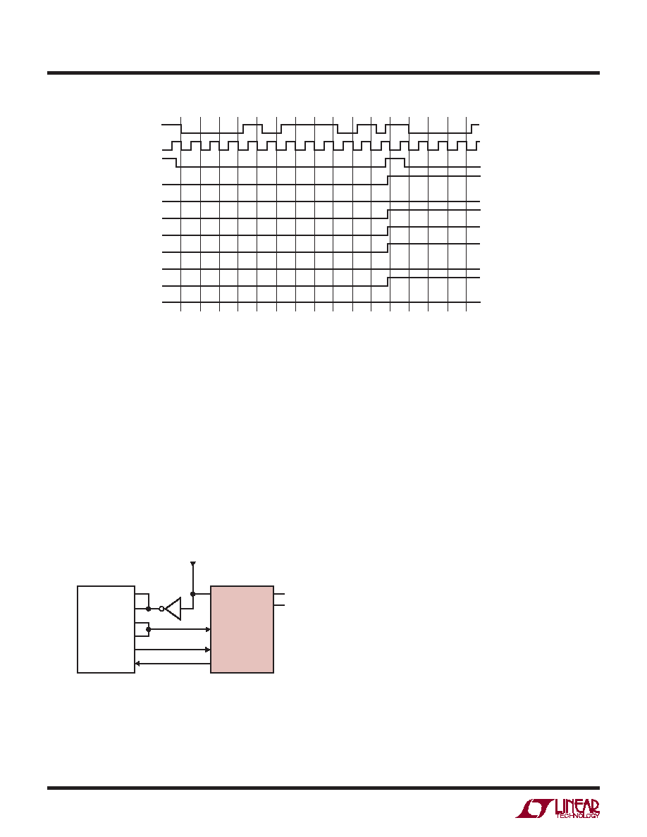
TYPICAL APPLICATIONS
Interfacing the LTC1198 to the TMS320C25 DSP
Figure 15 illustrates the interface between the LTC1198
8-bit data acquisition system and the TMS320C25 digital
signal processor (DSP). The interface, which is optimized
for speed of transfer and minimum processor supervision,
can complete a conversion and shift the data in 4μs with
fCLK = 5MHz. The cycle time, 4μs, of each conversion is
limited by maximum clock frequency of the serial port of
the TMS320C25 which is 5MHz. The supply voltage for
the LTC1198 in Figure 15 can be 2.7V to 6V with fCLK =
5MHz. At 2.7V, fCLK = 5MHz will work at 25°C. See the
Recommended Operating Conditions table in the Electrical
Characteristics section for limits over temperature.
Hardware Description
The circuit works as follows: the LTC1198 clock line
controls the A/D conversion rate and the data shift rate.
Data is transferred in a synchronous format over DIN and
DOUT. The serial port of the TMS320C25 is compatible
with that of the LTC1198. The data shift clock lines (CLKR,
CLKX) are inputs only. The data shift clock comes from
an external source. Inverting the shift clock is necessary
because the LTC1198 and the TMS320C25 clock the input
data on opposite edges.
The schematic of Figure 15 is fed by an external clock
source. The signal is fed into the CLK pin of the LTC1198
directly. The signal is inverted with a 74HC04 and then
applied to the data shift clock lines (CLKR, CLKX). The
framing pulse of the TMS320C25 is fed directly to the CS
of the LTC1198. DX and DR are tied directly to DIN and
DOUT, respectively.
70
140
210
280
350
420
490
560
630
700
770
840
910
980 1050 1120
DATA
CLK
CS
B7
B4
B6
B5
B3
B1
B2
B0
TIME (ns)
1196/98 F14
Figure 14. The Timing Diagram
1196/98 F15
5MHz CLK
CLKX
CLKR
FSR
FSX
DX
DR
CLK
LTC1198
TMS320C25
CS
DIN
DOUT
CH0
CH1
Figure 15. Interfacing the LTC1198 to the TMS320C25 DSP
相关PDF资料 |
PDF描述 |
|---|---|
| LTC1257IS8#TRPBF | IC D/A CONV 12BIT VOLT OUT 8SOIC |
| LTC1276ACN#PBF | IC A/D CONV 12BIT SAMPLING 24DIP |
| LTC1278-4IN#PBF | IC A/DCONV SAMPLNG W/SHTDN 24DIP |
| LTC1279CG#TRPBF | IC A/DCONV SAMPLNG W/SHTDN24SSOP |
| LTC1282ACN#PBF | IC A/D CONV SAMPLING W/REF 24DIP |
相关代理商/技术参数 |
参数描述 |
|---|---|
| LTC1198-1BCS8-TRPBF | 制造商:LINER 制造商全称:Linear Technology 功能描述:8-Bit, SO-8, 1Msps ADCs with Auto-Shutdown Options |
| LTC1198-2AC | 制造商:LINER 制造商全称:Linear Technology 功能描述:8-Bit, SO-8, 1MSPS ADCs with Auto-Shutdown Options |
| LTC1198-2ACS8 | 功能描述:IC ADC 8BIT 750KHZ SAMPL 8-SOIC RoHS:否 类别:集成电路 (IC) >> 数据采集 - 模数转换器 系列:- 其它有关文件:TSA1204 View All Specifications 标准包装:1 系列:- 位数:12 采样率(每秒):20M 数据接口:并联 转换器数目:2 功率耗散(最大):155mW 电压电源:模拟和数字 工作温度:-40°C ~ 85°C 安装类型:表面贴装 封装/外壳:48-TQFP 供应商设备封装:48-TQFP(7x7) 包装:Digi-Reel® 输入数目和类型:4 个单端,单极;2 个差分,单极 产品目录页面:1156 (CN2011-ZH PDF) 其它名称:497-5435-6 |
| LTC1198-2ACS8#PBF | 功能描述:IC ADC 8BIT 750KHZ SAMPL 8-SOIC RoHS:是 类别:集成电路 (IC) >> 数据采集 - 模数转换器 系列:- 产品培训模块:Lead (SnPb) Finish for COTS Obsolescence Mitigation Program 标准包装:2,500 系列:- 位数:12 采样率(每秒):3M 数据接口:- 转换器数目:- 功率耗散(最大):- 电压电源:- 工作温度:- 安装类型:表面贴装 封装/外壳:SOT-23-6 供应商设备封装:SOT-23-6 包装:带卷 (TR) 输入数目和类型:- |
| LTC1198-2ACS8#TR | 功能描述:IC ADC 8BIT 750KHZ SHUTDWN 8SOIC RoHS:否 类别:集成电路 (IC) >> 数据采集 - 模数转换器 系列:- 标准包装:2,500 系列:- 位数:16 采样率(每秒):15 数据接口:MICROWIRE?,串行,SPI? 转换器数目:1 功率耗散(最大):480µW 电压电源:单电源 工作温度:-40°C ~ 85°C 安装类型:表面贴装 封装/外壳:38-WFQFN 裸露焊盘 供应商设备封装:38-QFN(5x7) 包装:带卷 (TR) 输入数目和类型:16 个单端,双极;8 个差分,双极 配用:DC1011A-C-ND - BOARD DELTA SIGMA ADC LTC2494 |
发布紧急采购,3分钟左右您将得到回复。