- 您现在的位置:买卖IC网 > PDF目录15253 > LTC1266CS-3.3 (Linear Technology)IC REG CTRLR BST PWM CM 16-SOIC PDF资料下载
参数资料
| 型号: | LTC1266CS-3.3 |
| 厂商: | Linear Technology |
| 文件页数: | 14/20页 |
| 文件大小: | 0K |
| 描述: | IC REG CTRLR BST PWM CM 16-SOIC |
| 标准包装: | 50 |
| PWM 型: | 电流模式 |
| 输出数: | 1 |
| 频率 - 最大: | 400kHz |
| 占空比: | 100% |
| 电源电压: | 3.5 V ~ 18 V |
| 降压: | 是 |
| 升压: | 是 |
| 回扫: | 无 |
| 反相: | 无 |
| 倍增器: | 无 |
| 除法器: | 无 |
| Cuk: | 无 |
| 隔离: | 无 |
| 工作温度: | 0°C ~ 70°C |
| 封装/外壳: | 16-SOIC(0.154",3.90mm 宽) |
| 包装: | 管件 |
| 产品目录页面: | 1342 (CN2011-ZH PDF) |
�� �
�
�LTC1266�
�LTC1266-3.3/LTC1266-5�
�APPLICATIO� S� I� FOR� ATIO�
�discharge� C� OUT� until� the� regulator� loop� adapts� to� the�
�current� change� and� returns� V� OUT� to� its� steady-state� value.�
�During� this� recovery� time� V� OUT� can� be� monitored� for�
�overshoot� or� ringing� which� would� indicate� a� stability�
�problem.� The� Pin� 7� external� components� shown� in� the�
�Figure� 1� circuit� will� prove� adequate� compensation� for�
�most� applications.�
�Efficiency� Considerations�
�The� percent� efficiency� of� a� switching� regulator� is� equal� to�
�the� output� power� divided� by� the� input� power� times� 100%.�
�It� is� often� useful� to� analyze� individual� losses� to� determine�
�what� is� limiting� the� efficiency� and� which� change� would�
�produce� the� most� improvement.� Percent� efficiency� can� be�
�expressed� as:�
�%� Efficiency� =� 100%� –� (L1� +� L2� +� L3� +� ...)�
�where� L1,� L2,� etc.,� are� the� individual� losses� as� a� percent-�
�age� of� input� power.� (For� high� efficiency� circuits,� only� small�
�errors� are� incurred� by� expressing� losses� as� a� percentage�
�of� output� power).�
�Although� all� dissipative� elements� in� the� circuit� produce�
�losses,� three� main� sources� usually� account� for� most� of� the�
�losses� in� LTC1266� series� circuits:� 1)� LTC1266� DC� bias�
�current,� 2)� MOSFET� gate� charge� current� and� 3)� I� 2� R� losses.�
�1.� The� DC� supply� current� is� the� current� which� flows� into�
�V� IN� (Pin� 2).� For� V� IN� =� 10V� the� LTC1266� DC� supply� current�
�is� 170� μ� A� for� no� load,� and� increases� proportionally� with�
�load� up� to� a� constant� 2.1mA� after� the� LTC1266� series� has�
�entered� continuous� mode.� Because� the� DC� bias� current� is�
�15nC.� This� results� in� I� GATECHG� =� 6mA� in� 200kHz� continu-�
�ous� operation� for� a� 2%� to� 3%� typical� mid-current� loss� with�
�V� IN� =� 5V.�
�Note� that� the� gate� charge� loss� increases� directly� with�
�both� input� voltage� and� operating� frequency.� This� is� the�
�principal� reason� why� the� highest� efficiency� circuits� oper-�
�ate� at� moderate� frequencies.� Furthermore,� it� argues� against�
�using� larger� MOSFETs� than� necessary� to� control� I� 2� R�
�losses,� since� overkill� can� cost� efficiency� as� well� as� money!�
�3.� I� 2� R� losses� are� easily� predicted� from� the� DC� resistances�
�of� the� MOSFET,� inductor� and� current� shunt.� In� continuous�
�mode� the� average� output� current� flows� through� L� and�
�R� SENSE� ,� but� is� “chopped”� between� the� topside� and� bot-�
�tom-side� MOSFETs.� If� the� two� MOSFETs� have� approxi-�
�mately� the� same� R� DS(ON)� ,� then� the� resistance� of� one�
�MOSFET� can� simply� be� summed� with� the� resistances� of� L�
�and� R� SENSE� to� obtain� I� 2� R� losses.� For� example,� if� each�
�R� DS(ON)� =� 0.05� ?� ,� R� L� =� 0.05� ?� and� R� SENSE� =� 0.02� ?� ,� then�
�the� total� resistance� is� 0.12� ?� .� This� results� in� losses� ranging�
�from� 3.5%� to� 15%� as� the� output� current� increases� from� 1A�
�to� 5A.� I� 2� R� losses� cause� the� efficiency� to� roll� off� at� high�
�output� currents.�
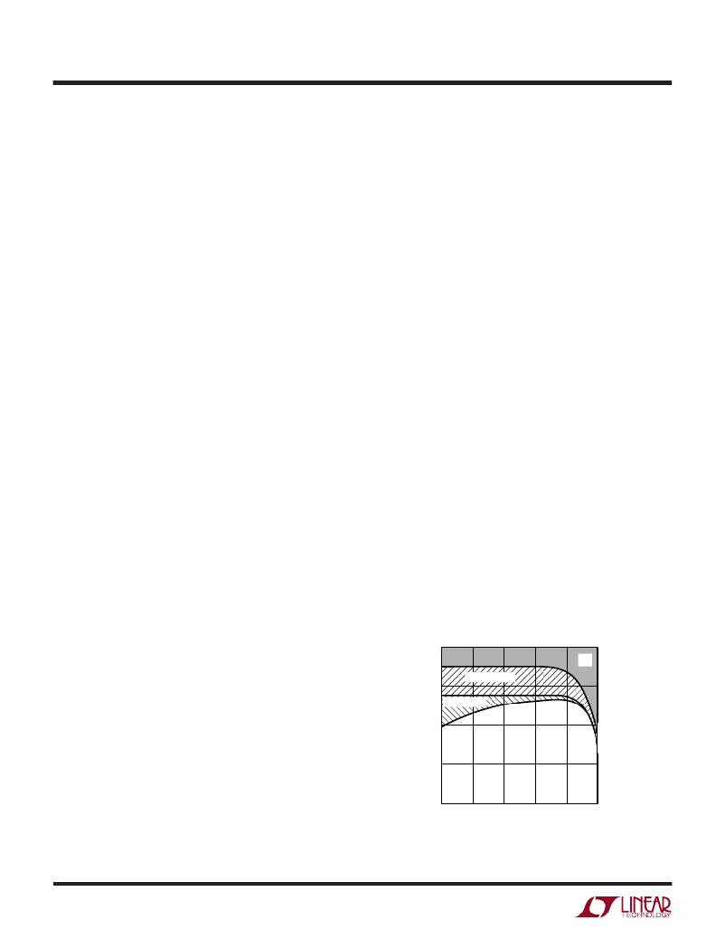
�Figure� 8� shows� how� the� efficiency� losses� in� a� typical�
�LTC1266� series� regulator� end� up� being� apportioned.� The�
�gate� charge� loss� is� responsible� for� the� majority� of� the�
�efficiency� lost� in� the� mid-current� region.� If� Burst� Mode�
�operation� was� not� employed� at� low� currents,� the� gate�
�charge� loss� alone� would� cause� efficiency� to� drop� to�
�unacceptable� levels� (see� Figure� 7).� With� Burst� Mode�
�drawn� from� V� IN� ,� the� resulting� loss� increases� with� input�
�voltage.� For� V� IN� =� 5V� the� DC� bias� losses� are� generally� less�
�than� 1%� for� load� currents� over� 30mA.� However,� at� very�
�low� load� currents� the� DC� bias� current� accounts� for� nearly�
�100�
�95�
�GATE CHARGE�
�LTC1266� I� Q�
�I� 2� R�
�all� of� the� loss.�
�90�
�2.� MOSFET� gate� charge� current� results� from� switching� the�
�gate� capacitance� of� the� power� MOSFETs.� Each� time� a�
�MOSFET� gate� is� switched� from� low� to� high� to� low� again,� a�
�packet� of� charge� dQ� moves� from� Power� V� IN� to� ground.� The�
�85�
�resulting� dQ/dt� is� a� current� flowing� into� Power� V� IN� (Pin� 5)�
�which� is� typically� much� larger� than� the� DC� supply� current.�
�80�
�0.01�
�0.03�
�0.1� 0.3�
�I� OUT� (A)�
�1�
�5�
�In� continuous� mode,� I� GATECHG� =� f� (Q� N� +� Q� P� ).� The� typical�
�gate� charge� for� a� 0.05� ?� N-channel� power� MOSFET� is�
�14�
�Figure� 8.� Efficiency� Loss�
�1266� F08�
�相关PDF资料 |
PDF描述 |
|---|---|
| VE-B7Y-EW-F3 | CONVERTER MOD DC/DC 3.3V 66W |
| RMM15DRMN-S288 | CONN EDGECARD 30POS .156 EXTEND |
| GBC25DRAS-S734 | CONN EDGECARD 50POS .100 R/A SLD |
| UCA2W220MHD | CAP ALUM 22UF 450V 20% RADIAL |
| LT3781EG#TRPBF | IC REG CTRLR ISO PWM CM 20-SSOP |
相关代理商/技术参数 |
参数描述 |
|---|---|
| LTC1266CS-5 | 功能描述:IC REG CTRLR BST PWM CM 16-SOIC RoHS:否 类别:集成电路 (IC) >> PMIC - 稳压器 - DC DC 切换控制器 系列:- 标准包装:2,500 系列:- PWM 型:电流模式 输出数:1 频率 - 最大:500kHz 占空比:96% 电源电压:4 V ~ 36 V 降压:无 升压:是 回扫:无 反相:无 倍增器:无 除法器:无 Cuk:无 隔离:无 工作温度:-40°C ~ 125°C 封装/外壳:24-WQFN 裸露焊盘 包装:带卷 (TR) |
| LTC1266CS-5#PBF | 功能描述:IC REG CTRLR BST PWM CM 16-SOIC RoHS:是 类别:集成电路 (IC) >> PMIC - 稳压器 - DC DC 切换控制器 系列:- 标准包装:2,500 系列:- PWM 型:电流模式 输出数:1 频率 - 最大:500kHz 占空比:96% 电源电压:4 V ~ 36 V 降压:无 升压:是 回扫:无 反相:无 倍增器:无 除法器:无 Cuk:无 隔离:无 工作温度:-40°C ~ 125°C 封装/外壳:24-WQFN 裸露焊盘 包装:带卷 (TR) |
| LTC1266CS-5#TR | 功能描述:IC REG CTRLR BST PWM CM 16-SOIC RoHS:否 类别:集成电路 (IC) >> PMIC - 稳压器 - DC DC 切换控制器 系列:- 标准包装:2,500 系列:- PWM 型:电流模式 输出数:1 频率 - 最大:500kHz 占空比:96% 电源电压:4 V ~ 36 V 降压:无 升压:是 回扫:无 反相:无 倍增器:无 除法器:无 Cuk:无 隔离:无 工作温度:-40°C ~ 125°C 封装/外壳:24-WQFN 裸露焊盘 包装:带卷 (TR) |
| LTC1266CS-5#TRPBF | 功能描述:IC REG CTRLR BST PWM CM 16-SOIC RoHS:否 类别:集成电路 (IC) >> PMIC - 稳压器 - DC DC 切换控制器 系列:- 标准包装:2,500 系列:- PWM 型:电流模式 输出数:1 频率 - 最大:500kHz 占空比:96% 电源电压:4 V ~ 36 V 降压:无 升压:是 回扫:无 反相:无 倍增器:无 除法器:无 Cuk:无 隔离:无 工作温度:-40°C ~ 125°C 封装/外壳:24-WQFN 裸露焊盘 包装:带卷 (TR) |
| LTC1266IS | 功能描述:IC REG CTRLR BST PWM CM 16-SOIC RoHS:否 类别:集成电路 (IC) >> PMIC - 稳压器 - DC DC 切换控制器 系列:- 标准包装:2,500 系列:- PWM 型:电流模式 输出数:1 频率 - 最大:500kHz 占空比:96% 电源电压:4 V ~ 36 V 降压:无 升压:是 回扫:无 反相:无 倍增器:无 除法器:无 Cuk:无 隔离:无 工作温度:-40°C ~ 125°C 封装/外壳:24-WQFN 裸露焊盘 包装:带卷 (TR) |
发布紧急采购,3分钟左右您将得到回复。