- 您现在的位置:买卖IC网 > PDF目录80088 > LTC1266CS#TR-5 (LINEAR TECHNOLOGY CORP) SWITCHING CONTROLLER, 400 kHz SWITCHING FREQ-MAX, PDSO16 PDF资料下载
参数资料
| 型号: | LTC1266CS#TR-5 |
| 厂商: | LINEAR TECHNOLOGY CORP |
| 元件分类: | 稳压器 |
| 英文描述: | SWITCHING CONTROLLER, 400 kHz SWITCHING FREQ-MAX, PDSO16 |
| 封装: | 0.150 INCH, PLASTIC, SO-16 |
| 文件页数: | 4/20页 |
| 文件大小: | 245K |
| 代理商: | LTC1266CS#TR-5 |
12
LTC1266
LTC1266-3.3/LTC1266-5
Driving N-Channel Topside MOSFETs
Driving an N-channel topside MOSFET (PINV, Pin 3, tied to
PWR VIN) is a little trickier than driving a P-channel since
the gate voltage must be positive with respect to the
source to turn it on, which means that the gate voltage
must be higher than VIN. This requires either a second
supply at least VGS(ON) above VIN or a bootstrapping circuit
to boost the VIN to the proper level. The easiest method is
using a higher supply (see Figure 14) but if one is not
available, the bootstrap method can be used at the ex-
pense of an additional diode (see Figure 1). The bootstrap
works by charging the bootstrap capacitor to VIN during
the off-time. During the on-time, the bottom plate of the
capacitor is pulled up to VIN so that the voltage at Pin 2 is
now twice VIN (plus any ringing on the switch node).
Since the maximum allowable voltage at Pin 2 is 20V, the
Figure 1 bootstrap circuit limits VIN to less than 10V. A
higher VIN can be achieved if the bootstrap capacitor is
charged to a voltage less than VIN, in which case
VIN(MAX) = 20 – VCAP.
N-channel mode, internal circuitry limits the maximum
on-time to 60
s to guarantee start-up of the bootstrap
circuit. This maximum on-time reduces the maximum
duty cycle to:
Max Duty Cycle =
60
s
60
s + tOFF
which slightly increases the minimum input voltage at
which dropout occurs. However, because of the superior
on-conductance of the N-channel, the dropout perfor-
mance of an all N-channel regulator is still better (see
Figure 5) even with the duty cycle limitation, except at light
loads.
Low-Battery Comparator
The LTC1266 has an on-chip low-battery comparator
which can be used to sense a low-battery condition when
implemented as shown in Figure 6. The resistor divider
R1, R2 sets the comparator trip point as follows:
VTRIP = 1.25
)
)1+ R2
R1
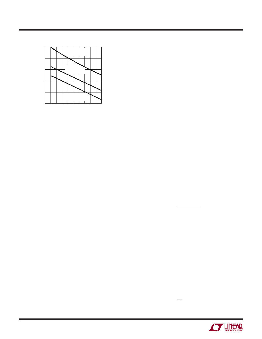
(VIN – VOUT) VOLTAGE (V)
0
C
OUT
(
F) 600
800
1000
4
1266 F04
400
200
0
1
2
3
5
L = 50
H
RSENSE = 0.02
L = 25
H
RSENSE = 0.02
L = 50
H
RSENSE = 0.05
Figure 4. Minimum Value of COUT
series would normally be in continuous operation. The
output remains in regulation at all times. This minimum
capacitance requirement may be relaxed if Burst Mode
operation is disabled.
N-Channel vs P-Channel MOSFETs
The LTC1266 has the capability to drive either an
N-channel or a P-channel topside switch to give the user
more flexibility. N-channel MOSFETs are superior in per-
formance to P-channel due to their lower RDS(ON) and
lower gate capacitance and are typically less expensive;
however, they do have a slightly more complicated gate
drive requirement and a more limited input voltage range
(see following sections).
Driving P-Channel Topside MOSFETs
The P-channel topside switch circuit configuration is the
most straightforward due to the requirement of only one
supply voltage level. This is due to the negative gate
threshold of the P-channel MOSFET which allows the
MOSFET to be switched on and off by swinging the gate
between VIN and ground. The phase invert (Pin 3) is tied
to ground to choose this operating mode. Normally, the
converter input (VIN) is connected to the LTC1266 supply
Pins 2 and 5 and can go as high as 20V. Pin 2 supplies the
high frequency current pulses to switch the MOSFETs and
should be decoupled with a 0.1
F to 1F ceramic capaci-
tor. Pin 5 supplies most of the quiescent power to the rest
of the chip.
APPLICATIO S I FOR ATIO
WU
UU
相关PDF资料 |
PDF描述 |
|---|---|
| LM1301-7ERV2AH | 1-OUTPUT 50 W AC-DC REG PWR SUPPLY MODULE |
| LM1301-9RV3 | 1-OUTPUT 50 W AC-DC REG PWR SUPPLY MODULE |
| LM1501-7ERV2F | 1-OUTPUT 50 W AC-DC REG PWR SUPPLY MODULE |
| LM1601-7EPV2H | 1-OUTPUT 50 W AC-DC REG PWR SUPPLY MODULE |
| LM1601-9EPV0HF | 1-OUTPUT 50 W AC-DC REG PWR SUPPLY MODULE |
相关代理商/技术参数 |
参数描述 |
|---|---|
| LTC1266IS | 功能描述:IC REG CTRLR BST PWM CM 16-SOIC RoHS:否 类别:集成电路 (IC) >> PMIC - 稳压器 - DC DC 切换控制器 系列:- 标准包装:2,500 系列:- PWM 型:电流模式 输出数:1 频率 - 最大:500kHz 占空比:96% 电源电压:4 V ~ 36 V 降压:无 升压:是 回扫:无 反相:无 倍增器:无 除法器:无 Cuk:无 隔离:无 工作温度:-40°C ~ 125°C 封装/外壳:24-WQFN 裸露焊盘 包装:带卷 (TR) |
| LTC1266IS#PBF | 功能描述:IC REG CTRLR BST PWM CM 16-SOIC RoHS:是 类别:集成电路 (IC) >> PMIC - 稳压器 - DC DC 切换控制器 系列:- 标准包装:2,500 系列:- PWM 型:电流模式 输出数:1 频率 - 最大:500kHz 占空比:96% 电源电压:4 V ~ 36 V 降压:无 升压:是 回扫:无 反相:无 倍增器:无 除法器:无 Cuk:无 隔离:无 工作温度:-40°C ~ 125°C 封装/外壳:24-WQFN 裸露焊盘 包装:带卷 (TR) |
| LTC1266IS#TR | 功能描述:IC REG CTRLR BST PWM CM 16-SOIC RoHS:否 类别:集成电路 (IC) >> PMIC - 稳压器 - DC DC 切换控制器 系列:- 标准包装:2,500 系列:- PWM 型:电流模式 输出数:1 频率 - 最大:500kHz 占空比:96% 电源电压:4 V ~ 36 V 降压:无 升压:是 回扫:无 反相:无 倍增器:无 除法器:无 Cuk:无 隔离:无 工作温度:-40°C ~ 125°C 封装/外壳:24-WQFN 裸露焊盘 包装:带卷 (TR) |
| LTC1266IS#TRPBF | 功能描述:IC REG CTRLR BST PWM CM 16-SOIC RoHS:是 类别:集成电路 (IC) >> PMIC - 稳压器 - DC DC 切换控制器 系列:- 标准包装:2,500 系列:- PWM 型:电流模式 输出数:1 频率 - 最大:500kHz 占空比:96% 电源电压:4 V ~ 36 V 降压:无 升压:是 回扫:无 反相:无 倍增器:无 除法器:无 Cuk:无 隔离:无 工作温度:-40°C ~ 125°C 封装/外壳:24-WQFN 裸露焊盘 包装:带卷 (TR) |
| LTC1266IS-3.3 | 功能描述:IC REG CTRLR BST PWM CM 16-SOIC RoHS:否 类别:集成电路 (IC) >> PMIC - 稳压器 - DC DC 切换控制器 系列:- 标准包装:2,000 系列:- PWM 型:电流模式 输出数:1 频率 - 最大:1MHz 占空比:50% 电源电压:9 V ~ 10 V 降压:无 升压:是 回扫:是 反相:无 倍增器:无 除法器:无 Cuk:无 隔离:无 工作温度:-40°C ~ 85°C 封装/外壳:8-TSSOP(0.173",4.40mm 宽) 包装:带卷 (TR) |
发布紧急采购,3分钟左右您将得到回复。