- 您现在的位置:买卖IC网 > PDF目录10534 > LTC1282BCN (Linear Technology)IC A/D CONV SAMPLING W/REF 24DIP PDF资料下载
参数资料
| 型号: | LTC1282BCN |
| 厂商: | Linear Technology |
| 文件页数: | 6/24页 |
| 文件大小: | 0K |
| 描述: | IC A/D CONV SAMPLING W/REF 24DIP |
| 标准包装: | 15 |
| 位数: | 12 |
| 采样率(每秒): | 140k |
| 数据接口: | 并联 |
| 转换器数目: | 1 |
| 功率耗散(最大): | 24mW |
| 电压电源: | 双 ± |
| 工作温度: | 0°C ~ 70°C |
| 安装类型: | 通孔 |
| 封装/外壳: | 24-DIP(0.300",7.62mm) |
| 供应商设备封装: | 24-PDIP |
| 包装: | 管件 |
| 输入数目和类型: | 1 个单端,单极;1 个单端,双极 |
14
LTC1282
U
S
A
O
PPLICATI
WU
U
I FOR ATIO
offset, apply 0.305mV (i.e., 0.5LSB) at V1 and adjust the
op amp offset voltage until the LTC1282 output code
flickers between 0000 0000 0000 and 0000 0000 0001.
For zero full-scale error, apply an analog input of 2.49909V
(i.e., FS – 1.5LSBs or last code transition) at the input and
adjust the full-scale trim until the LTC1282 output code
flickers between 1111 1111 1110 and 1111 1111 1111.
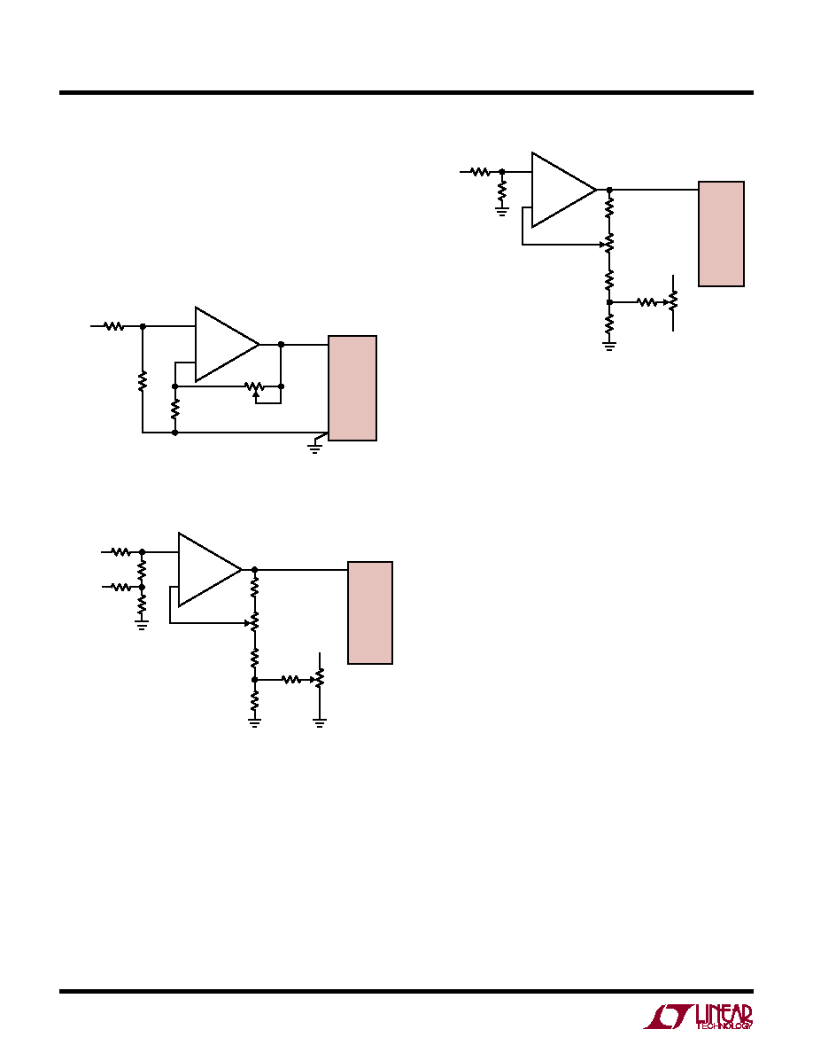
Figure 10. Full-Scale Adjust Circuit
Figure 11. Unipolar Offset and Full-Scale Adjust Circuit
Figure 12. Bipolar Offset and Full-Scale Adjust Circuit
error adjustment is achieved by trimming the offset ad-
justment of Figure 12 while the input voltage is 0.5LSB
below ground. This is done by applying an input voltage of
– 0.305mV (– 0.5LSB for LTC1282) to the input in Figure
12 and adjusting R8 until the ADC output code flickers
between 0000 0000 0000 and 1111 1111 1111. For full-
scale adjustment, an input voltage of 1.24909V (FS –
1.5LSBs for LTC1282) is applied to the input and R5 is
adjusted until the output code flickers between 0111 1111
1110 and 0111 1111 1111.
BOARD LAYOUT AND BYPASSING
The LTC1282 is easy to use. To obtain the best perfor-
mance from the device, a printed circuit board is recom-
mended. Layout for the printed circuit board should en-
sure that digital and analog signal lines are separated as
much as possible. In particular, care should be taken not
to run any digital track alongside an analog signal track or
underneath the ADC. The analog input should be screened
by AGND.
High quality tantalum and ceramic bypass capacitors
should be used at the VDD and VREF pins as shown in Figure
13. In bipolar mode, a 0.1
F ceramic provides adequate
bypassing for the VSS pin. The capacitors must be located
as close to the pins as possible. The traces connecting the
pins and the bypass capacitors must be kept short and
should be made as wide as possible.
Bipolar Offset and Full-Scale Adjustment
Bipolar offset and full-scale errors are adjusted in a
similar fashion to the unipolar case. Figure 10 shows the
extra components required for full-scale error adjust-
ment. If both offset and full-scale adjustments are needed,
the circuit in Figure 12 can be used. Again, bipolar offset
must be adjusted before full-scale error. Bipolar offset
LTC1282
AIN
AGND
LTC1282 F10
R4
100
FULL-SCALE
ADJUST
R5
10k
R2
10k
R1
50
V1
–
+
A1
ADDITIONAL PINS OMITTED FOR CLARITY
±20LSB TRIM RANGE
AIN
LTC1282 F11
R2
10k
R4
100k
R1
10k
5V
R9
20
ANALOG
INPUT
0V TO 2.5V
R3
100k
5V
R8
10k
OFFSET
ADJUST
R6
400
R5
4.3k
FULL-SCALE
ADJUST
R7
100k
–
+
LTC1282
AIN
LTC1282 F12
R2
10k
R4
100k
R1
10k
ANALOG
INPUT
±1.25V
R3
100k
5V
R8
20k
OFFSET
ADJUST
R6
200
R5
4.3k
FULL-SCALE
ADJUST
R7
100k
–
+
LTC1282
–5V
相关PDF资料 |
PDF描述 |
|---|---|
| VE-242-IW-F1 | CONVERTER MOD DC/DC 15V 100W |
| VI-JWZ-MW-F2 | CONVERTER MOD DC/DC 2V 40W |
| AD9600ABCPZ-105 | IC ADC 10BIT 105MSPS 64LFCSP |
| VE-241-IW-F3 | CONVERTER MOD DC/DC 12V 100W |
| AD7653ACPZ | IC ADC 16BIT UNIPOLAR 48LFCSP |
相关代理商/技术参数 |
参数描述 |
|---|---|
| LTC1282BCN#PBF | 功能描述:IC A/D CONV SAMPLING W/REF 24DIP RoHS:是 类别:集成电路 (IC) >> 数据采集 - 模数转换器 系列:- 产品培训模块:Lead (SnPb) Finish for COTS Obsolescence Mitigation Program 标准包装:2,500 系列:- 位数:12 采样率(每秒):3M 数据接口:- 转换器数目:- 功率耗散(最大):- 电压电源:- 工作温度:- 安装类型:表面贴装 封装/外壳:SOT-23-6 供应商设备封装:SOT-23-6 包装:带卷 (TR) 输入数目和类型:- |
| LTC1282BCSW | 功能描述:IC A/D CONV SAMPLING W/REF24SOIC RoHS:否 类别:集成电路 (IC) >> 数据采集 - 模数转换器 系列:- 标准包装:1,000 系列:- 位数:12 采样率(每秒):300k 数据接口:并联 转换器数目:1 功率耗散(最大):75mW 电压电源:单电源 工作温度:0°C ~ 70°C 安装类型:表面贴装 封装/外壳:24-SOIC(0.295",7.50mm 宽) 供应商设备封装:24-SOIC 包装:带卷 (TR) 输入数目和类型:1 个单端,单极;1 个单端,双极 |
| LTC1282BCSW#PBF | 功能描述:IC A/D CONV SAMPLING W/REF24SOIC RoHS:是 类别:集成电路 (IC) >> 数据采集 - 模数转换器 系列:- 标准包装:1,000 系列:- 位数:12 采样率(每秒):300k 数据接口:并联 转换器数目:1 功率耗散(最大):75mW 电压电源:单电源 工作温度:0°C ~ 70°C 安装类型:表面贴装 封装/外壳:24-SOIC(0.295",7.50mm 宽) 供应商设备封装:24-SOIC 包装:带卷 (TR) 输入数目和类型:1 个单端,单极;1 个单端,双极 |
| LTC1282BCSW#TR | 功能描述:IC ADC 12BIT SAMPLING REF 24SOIC RoHS:否 类别:集成电路 (IC) >> 数据采集 - 模数转换器 系列:- 标准包装:1,000 系列:- 位数:12 采样率(每秒):300k 数据接口:并联 转换器数目:1 功率耗散(最大):75mW 电压电源:单电源 工作温度:0°C ~ 70°C 安装类型:表面贴装 封装/外壳:24-SOIC(0.295",7.50mm 宽) 供应商设备封装:24-SOIC 包装:带卷 (TR) 输入数目和类型:1 个单端,单极;1 个单端,双极 |
| LTC1282BCSW#TRPBF | 功能描述:IC A/D CONV SAMPLING W/REF24SOIC RoHS:是 类别:集成电路 (IC) >> 数据采集 - 模数转换器 系列:- 标准包装:1,000 系列:- 位数:12 采样率(每秒):300k 数据接口:并联 转换器数目:1 功率耗散(最大):75mW 电压电源:单电源 工作温度:0°C ~ 70°C 安装类型:表面贴装 封装/外壳:24-SOIC(0.295",7.50mm 宽) 供应商设备封装:24-SOIC 包装:带卷 (TR) 输入数目和类型:1 个单端,单极;1 个单端,双极 |
发布紧急采购,3分钟左右您将得到回复。