- 您现在的位置:买卖IC网 > PDF目录10534 > LTC1282BCN (Linear Technology)IC A/D CONV SAMPLING W/REF 24DIP PDF资料下载
参数资料
| 型号: | LTC1282BCN |
| 厂商: | Linear Technology |
| 文件页数: | 8/24页 |
| 文件大小: | 0K |
| 描述: | IC A/D CONV SAMPLING W/REF 24DIP |
| 标准包装: | 15 |
| 位数: | 12 |
| 采样率(每秒): | 140k |
| 数据接口: | 并联 |
| 转换器数目: | 1 |
| 功率耗散(最大): | 24mW |
| 电压电源: | 双 ± |
| 工作温度: | 0°C ~ 70°C |
| 安装类型: | 通孔 |
| 封装/外壳: | 24-DIP(0.300",7.62mm) |
| 供应商设备封装: | 24-PDIP |
| 包装: | 管件 |
| 输入数目和类型: | 1 个单端,单极;1 个单端,双极 |
16
LTC1282
U
S
A
O
PPLICATI
WU
U
I FOR ATIO
Internal Clock
The LTC1282 has an internal clock that eliminates the need
for synchronization between the external clock and the CS
and RD signals found in other ADCs. The internal clock is
factory trimmed to achieve a typical conversion time of
5.5
s, and a maximum conversion time over the full
operating temperature range of 6.0
s. No external adjust-
ments are required and, with the guaranteed maximum
acquisition time of 1.14
s, throughput performance of
140ksps is assured.
Timing and Control
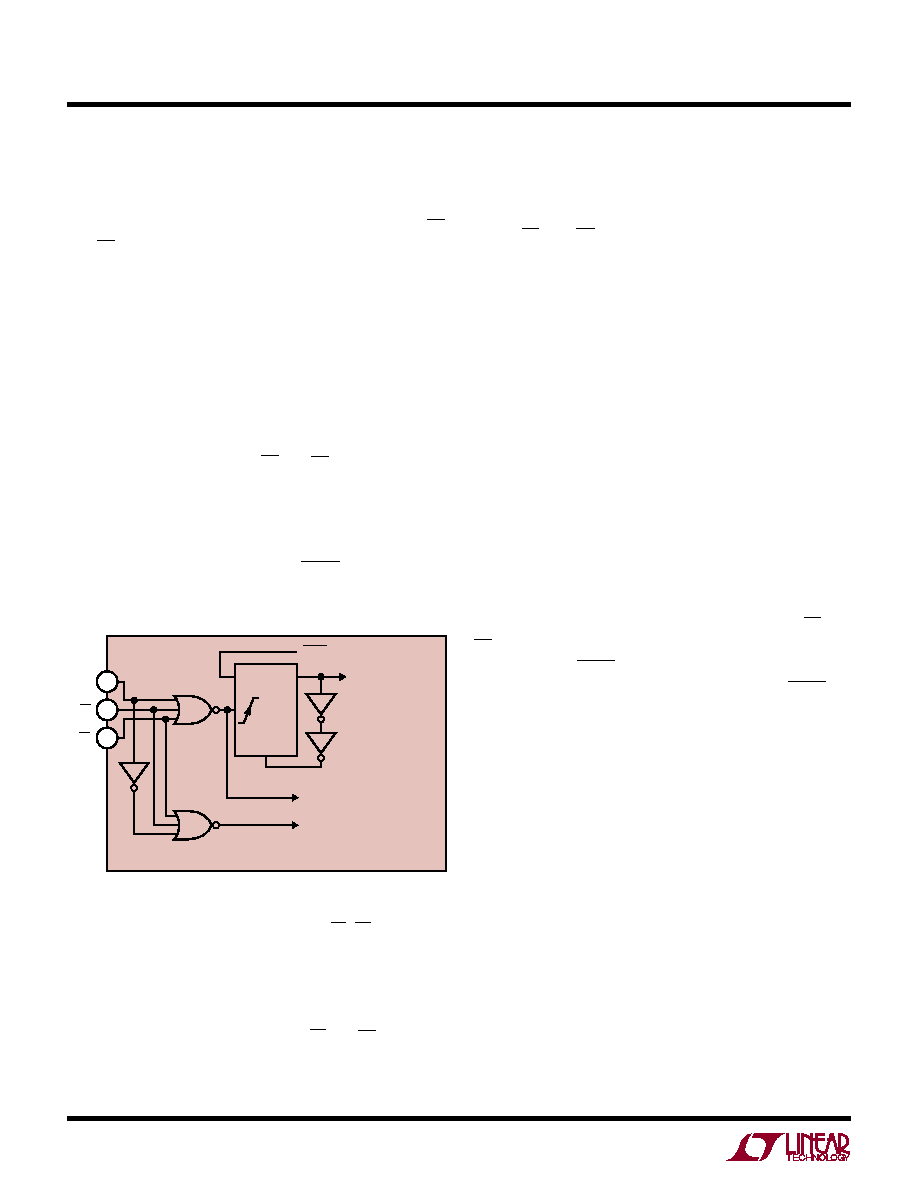
Conversion start and data read operations are controlled
by three digital inputs: HBEN, CS and RD. Figure 15 shows
the logic structure associated with these inputs. The three
signals are internally gated so that a logic “0” is required
on all three inputs to initiate a conversion. Once initiated it
cannot be restarted until the conversion is complete.
Converter status is indicated by the BUSY output, and this
is low while conversion is in progress.
initiates a conversion and data is read when conversion is
complete. The second is the ROM Mode which does not
require microprocessor WAIT states. A READ operation
brings CS and RD low which initiates a conversion and
reads the previous conversion result.
Data Format
The output format can be either a complete parallel load for
16-bit microprocessors or a two byte load for 8-bit micro-
processors. Data is always right justified (i.e., LSB is the
most right-hand bit in a 16-bit word). For a two byte read,
only data outputs D7...D0/8 are used. Byte selection is
governed by the HBEN input which controls an internal
digital multiplexer. This multiplexes the 12-bits of conver-
sion data onto the lower D7...D0/8 outputs (4MSBs or
8MSBs) where it can be read in two read cycles. The
4MSBs always appear on D11...D8 whenever the three-
state output drivers are turned on.
Slow Memory Mode, Parallel Read (HBEN = LOW)
Figure 16 and Table 2 show the timing diagram and data
bus status for Slow Memory Mode, Parallel Read. CS and
RD going low trigger a conversion and the ADC acknowl-
edges by taking BUSY low. Data from the previous conver-
sion appears on the three-state data outputs. BUSY re-
turns high at the end of conversion when the output
latches have been updated and the conversion result is
placed on data outputs D11...D0/8.
Slow Memory Mode, Two Byte Read
For a two byte read, only 8 data outputs D7...D0/8 are used.
Conversion start procedure and data output status for the
first read operation are identical to Slow Memory Mode,
Parallel Read. See Figure 17 timing diagram and Table 3
data bus status. At the end of the conversion, the low data
byte (D7...D0/8) is read from the ADC. A second READ
operation with the HBEN high, places the high byte on data
outputs D3/11...D0/8 and disables conversion start. Note
the 4MSBs appear on data output D11...D8 during the two
READ operations.
Figure 15. Internal Logic for Control Inputs CS, RD and HBEN
There are two modes of operation as outlined by the timing
diagrams of Figures 16 to 19. Slow Memory Mode is
designed for microprocessors which can be driven into a
WAIT state. A READ operation brings CS and RD low which
CONVERSION
START (RISING
EDGE TRIGGER)
LTC1282 F15
BUSY
FLIP
FLOP
CLEAR
Q
D
19
21
20
ACTIVE HIGH
ENABLE THREE-STATE OUTPUTS
D11....D0/8 = DB11....DB0
ENABLE THREE-STATE OUTPUTS
D11....D8 = DB11....DB8
D7....D4 = LOW
D3/11....D0/8 = DB11....DB8
HBEN
CS
RD
LTC1282
D11....D0/8 ARE THE ADC DATA OUTPUT PINS
DB11....DB0 ARE THE 12-BIT CONVERSION RESULTS
*
相关PDF资料 |
PDF描述 |
|---|---|
| VE-242-IW-F1 | CONVERTER MOD DC/DC 15V 100W |
| VI-JWZ-MW-F2 | CONVERTER MOD DC/DC 2V 40W |
| AD9600ABCPZ-105 | IC ADC 10BIT 105MSPS 64LFCSP |
| VE-241-IW-F3 | CONVERTER MOD DC/DC 12V 100W |
| AD7653ACPZ | IC ADC 16BIT UNIPOLAR 48LFCSP |
相关代理商/技术参数 |
参数描述 |
|---|---|
| LTC1282BCN#PBF | 功能描述:IC A/D CONV SAMPLING W/REF 24DIP RoHS:是 类别:集成电路 (IC) >> 数据采集 - 模数转换器 系列:- 产品培训模块:Lead (SnPb) Finish for COTS Obsolescence Mitigation Program 标准包装:2,500 系列:- 位数:12 采样率(每秒):3M 数据接口:- 转换器数目:- 功率耗散(最大):- 电压电源:- 工作温度:- 安装类型:表面贴装 封装/外壳:SOT-23-6 供应商设备封装:SOT-23-6 包装:带卷 (TR) 输入数目和类型:- |
| LTC1282BCSW | 功能描述:IC A/D CONV SAMPLING W/REF24SOIC RoHS:否 类别:集成电路 (IC) >> 数据采集 - 模数转换器 系列:- 标准包装:1,000 系列:- 位数:12 采样率(每秒):300k 数据接口:并联 转换器数目:1 功率耗散(最大):75mW 电压电源:单电源 工作温度:0°C ~ 70°C 安装类型:表面贴装 封装/外壳:24-SOIC(0.295",7.50mm 宽) 供应商设备封装:24-SOIC 包装:带卷 (TR) 输入数目和类型:1 个单端,单极;1 个单端,双极 |
| LTC1282BCSW#PBF | 功能描述:IC A/D CONV SAMPLING W/REF24SOIC RoHS:是 类别:集成电路 (IC) >> 数据采集 - 模数转换器 系列:- 标准包装:1,000 系列:- 位数:12 采样率(每秒):300k 数据接口:并联 转换器数目:1 功率耗散(最大):75mW 电压电源:单电源 工作温度:0°C ~ 70°C 安装类型:表面贴装 封装/外壳:24-SOIC(0.295",7.50mm 宽) 供应商设备封装:24-SOIC 包装:带卷 (TR) 输入数目和类型:1 个单端,单极;1 个单端,双极 |
| LTC1282BCSW#TR | 功能描述:IC ADC 12BIT SAMPLING REF 24SOIC RoHS:否 类别:集成电路 (IC) >> 数据采集 - 模数转换器 系列:- 标准包装:1,000 系列:- 位数:12 采样率(每秒):300k 数据接口:并联 转换器数目:1 功率耗散(最大):75mW 电压电源:单电源 工作温度:0°C ~ 70°C 安装类型:表面贴装 封装/外壳:24-SOIC(0.295",7.50mm 宽) 供应商设备封装:24-SOIC 包装:带卷 (TR) 输入数目和类型:1 个单端,单极;1 个单端,双极 |
| LTC1282BCSW#TRPBF | 功能描述:IC A/D CONV SAMPLING W/REF24SOIC RoHS:是 类别:集成电路 (IC) >> 数据采集 - 模数转换器 系列:- 标准包装:1,000 系列:- 位数:12 采样率(每秒):300k 数据接口:并联 转换器数目:1 功率耗散(最大):75mW 电压电源:单电源 工作温度:0°C ~ 70°C 安装类型:表面贴装 封装/外壳:24-SOIC(0.295",7.50mm 宽) 供应商设备封装:24-SOIC 包装:带卷 (TR) 输入数目和类型:1 个单端,单极;1 个单端,双极 |
发布紧急采购,3分钟左右您将得到回复。