- 您现在的位置:买卖IC网 > PDF目录10199 > LTC1282BCSW#PBF (Linear Technology)IC A/D CONV SAMPLING W/REF24SOIC PDF资料下载
参数资料
| 型号: | LTC1282BCSW#PBF |
| 厂商: | Linear Technology |
| 文件页数: | 5/24页 |
| 文件大小: | 0K |
| 描述: | IC A/D CONV SAMPLING W/REF24SOIC |
| 标准包装: | 32 |
| 位数: | 12 |
| 采样率(每秒): | 140k |
| 数据接口: | 并联 |
| 转换器数目: | 1 |
| 功率耗散(最大): | 24mW |
| 电压电源: | 双 ± |
| 工作温度: | 0°C ~ 70°C |
| 安装类型: | 表面贴装 |
| 封装/外壳: | 24-SOIC(0.295",7.50mm 宽) |
| 供应商设备封装: | 24-SOIC |
| 包装: | 管件 |
| 输入数目和类型: | 1 个单端,单极;1 个单端,双极 |
13
LTC1282
U
S
A
O
PPLICATI
WU
U
I FOR ATIO
Overdriving the Internal Reference
The VREF pin can be driven above its normal value with a
DAC or other means to provide input span adjustment.
Figure 6 shows an LT1006 op amp driving the reference
pin. The VREF pin must be driven to at least 1.25V to
prevent conflict with the internal reference. The reference
should be driven to no more than 1.44V in unipolar mode
or 2.88V for bipolar mode to keep the input span within the
single 3V or
±3V supplies.
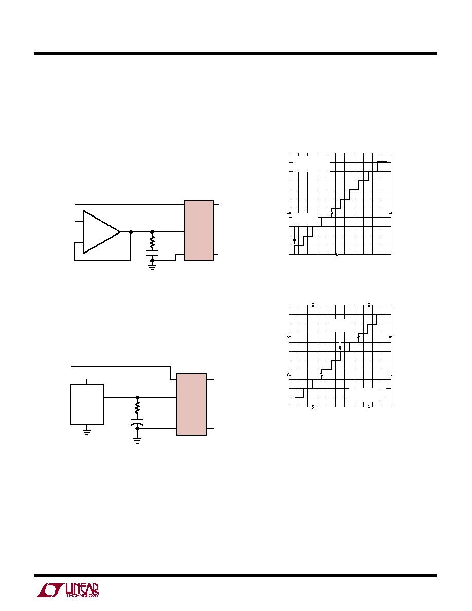
Figure 6. Driving the VREF with the LT1006 Op Amp
natural binary with 1LSB = FS/4096 = 2.5V/4096 = 0.61mV.
Figure 9 shows the input/output transfer characteristics
for the LTC1282 in bipolar operation. The full scale for
LTC1282 in bipolar mode is still 2.5V and 1LSB = 0.61mV.
UNIPOLAR/BIPOLAR OPERATION AND ADJUSTMENT
Figure 8 shows the ideal input/output characteristics for
the LTC1282. The code transitions occur midway be-
tween successive integer LSB values (i.e., 0.5LSB,
1.5LSBs, 2.5LSBs, FS – 1.5LSBs). The output code is
Figure 7. Supplying a 2.5V Reference Voltage
to the LTC1282 with the LT1019A-2.5
Figure 7 shows a typical reference, the LT1019A-2.5
connected to the LTC1282 operating in bipolar mode. This
will provide an improved drift (due to the 5ppm/
°C of the
LT1019A-2.5) and a
±2.604V full scale.
INPUT VOLTAGE (V)
0V
OUTPUT
CODE
FS – 1LSB
LTC1282 F8
111...111
111...110
111...101
111...100
000...000
000...001
000...010
000...011
1
LSB
UNIPOLAR
ZERO
1LSB = FS/4096
FS = 2.5V
Figure 8. LTC1282 Unipolar Transfer Characteristic
Figure 9. LTC1282 Bipolar Transfer Characteristic
Unipolar Offset and Full-Scale Adjustment
In applications where absolute accuracy is important,
offset and full-scale errors can be adjusted to zero. Figure
10 shows the extra components required for full-scale
error adjustment. If both offset and full-scale adjust-
ments are needed, the circuit in Figure 11 can be used.
Offset should be adjusted before full scale. To adjust
INPUT VOLTAGE (V)
0V
OUTPUT
CODE
–1
LSB
LTC1282 F09
011...111
011...110
000...001
000...000
100...000
100...001
100...010
1
LSB
BIPOLAR
ZERO
111...111
FS/2 – 1LSB
–FS/2
FS = 2.5V
1LSB = FS/4096
111...110
VREF(OUT) ≥ 1.25V
3
INPUT RANGE
±1.033VREF(OUT)
–
+
LT1006
10
F
LTC1282 F06
LTC1282
AIN
AGND
VREF
VDD
VSS
3V
–3V
3
INPUT RANGE
±2.60V
LTC1282
AIN
AGND
VREF
10
F
LTC1282 F07
LT1019A-2.5
VIN
GND
VOUT
5V
VDD
VSS
3V
–3V
+
相关PDF资料 |
PDF描述 |
|---|---|
| LTC1282BCSW | IC A/D CONV SAMPLING W/REF24SOIC |
| MS3106R-24-11S | CONN PLUG 9POS W/SOCKET SOLDER |
| CS6422-IS | IC CODEC SPKRPHONE 2CH 20-SOIC |
| AD9231BCPZRL7-40 | IC ADC 12BIT 40MSPS 64LFCSP |
| CS6422-CS | IC CODEC SPKRPHONE 2CH 20-SOIC |
相关代理商/技术参数 |
参数描述 |
|---|---|
| LTC1283ACN | 功能描述:IC DATA ACQ SYS 10BIT 3V 20-DIP RoHS:否 类别:集成电路 (IC) >> 数据采集 - ADCs/DAC - 专用型 系列:- 产品培训模块:Lead (SnPb) Finish for COTS Obsolescence Mitigation Program 标准包装:50 系列:- 类型:数据采集系统(DAS) 分辨率(位):16 b 采样率(每秒):21.94k 数据接口:MICROWIRE?,QSPI?,串行,SPI? 电压电源:模拟和数字 电源电压:1.8 V ~ 3.6 V 工作温度:-40°C ~ 85°C 安装类型:表面贴装 封装/外壳:40-WFQFN 裸露焊盘 供应商设备封装:40-TQFN-EP(6x6) 包装:托盘 |
| LTC1283ACN#PBF | 功能描述:IC DATA ACQ SYS 10BIT 3V 20-DIP RoHS:是 类别:集成电路 (IC) >> 数据采集 - ADCs/DAC - 专用型 系列:- 产品培训模块:Lead (SnPb) Finish for COTS Obsolescence Mitigation Program 标准包装:50 系列:- 类型:数据采集系统(DAS) 分辨率(位):16 b 采样率(每秒):21.94k 数据接口:MICROWIRE?,QSPI?,串行,SPI? 电压电源:模拟和数字 电源电压:1.8 V ~ 3.6 V 工作温度:-40°C ~ 85°C 安装类型:表面贴装 封装/外壳:40-WFQFN 裸露焊盘 供应商设备封装:40-TQFN-EP(6x6) 包装:托盘 |
| LTC1283CN | 功能描述:IC DATA ACQ SYS 10BIT 3V 20-DIP RoHS:否 类别:集成电路 (IC) >> 数据采集 - ADCs/DAC - 专用型 系列:- 产品培训模块:Lead (SnPb) Finish for COTS Obsolescence Mitigation Program 标准包装:50 系列:- 类型:数据采集系统(DAS) 分辨率(位):16 b 采样率(每秒):21.94k 数据接口:MICROWIRE?,QSPI?,串行,SPI? 电压电源:模拟和数字 电源电压:1.8 V ~ 3.6 V 工作温度:-40°C ~ 85°C 安装类型:表面贴装 封装/外壳:40-WFQFN 裸露焊盘 供应商设备封装:40-TQFN-EP(6x6) 包装:托盘 |
| LTC1283CN#PBF | 功能描述:IC DATA ACQ SYS 10BIT 3V 20-DIP RoHS:是 类别:集成电路 (IC) >> 数据采集 - ADCs/DAC - 专用型 系列:- 产品培训模块:Lead (SnPb) Finish for COTS Obsolescence Mitigation Program 标准包装:50 系列:- 类型:数据采集系统(DAS) 分辨率(位):16 b 采样率(每秒):21.94k 数据接口:MICROWIRE?,QSPI?,串行,SPI? 电压电源:模拟和数字 电源电压:1.8 V ~ 3.6 V 工作温度:-40°C ~ 85°C 安装类型:表面贴装 封装/外壳:40-WFQFN 裸露焊盘 供应商设备封装:40-TQFN-EP(6x6) 包装:托盘 |
| LTC1285CN8 | 功能描述:IC A/D CONV SAMPLING 12BIT 8-DIP RoHS:否 类别:集成电路 (IC) >> 数据采集 - 模数转换器 系列:- 标准包装:1,000 系列:- 位数:16 采样率(每秒):45k 数据接口:串行 转换器数目:2 功率耗散(最大):315mW 电压电源:模拟和数字 工作温度:0°C ~ 70°C 安装类型:表面贴装 封装/外壳:28-SOIC(0.295",7.50mm 宽) 供应商设备封装:28-SOIC W 包装:带卷 (TR) 输入数目和类型:2 个单端,单极 |
发布紧急采购,3分钟左右您将得到回复。