参数资料
| 型号: | LTC1289CCSW |
| 厂商: | Linear Technology |
| 文件页数: | 11/28页 |
| 文件大小: | 0K |
| 描述: | IC DATA ACQ SYS 12BIT 3V 20-SOIC |
| 标准包装: | 38 |
| 类型: | 数据采集系统(DAS) |
| 分辨率(位): | 12 b |
| 采样率(每秒): | 25k |
| 数据接口: | 串行,并联 |
| 电压电源: | 双 ± |
| 电源电压: | ±3.3V |
| 工作温度: | 0°C ~ 70°C |
| 安装类型: | 表面贴装 |
| 封装/外壳: | 20-SOIC(0.295",7.50mm 宽) |
| 供应商设备封装: | 20-SOIC |
| 包装: | 管件 |
| 其它名称: | LTC1289CCS |
第1页第2页第3页第4页第5页第6页第7页第8页第9页第10页当前第11页第12页第13页第14页第15页第16页第17页第18页第19页第20页第21页第22页第23页第24页第25页第26页第27页第28页
19
LTC1289
1289fb
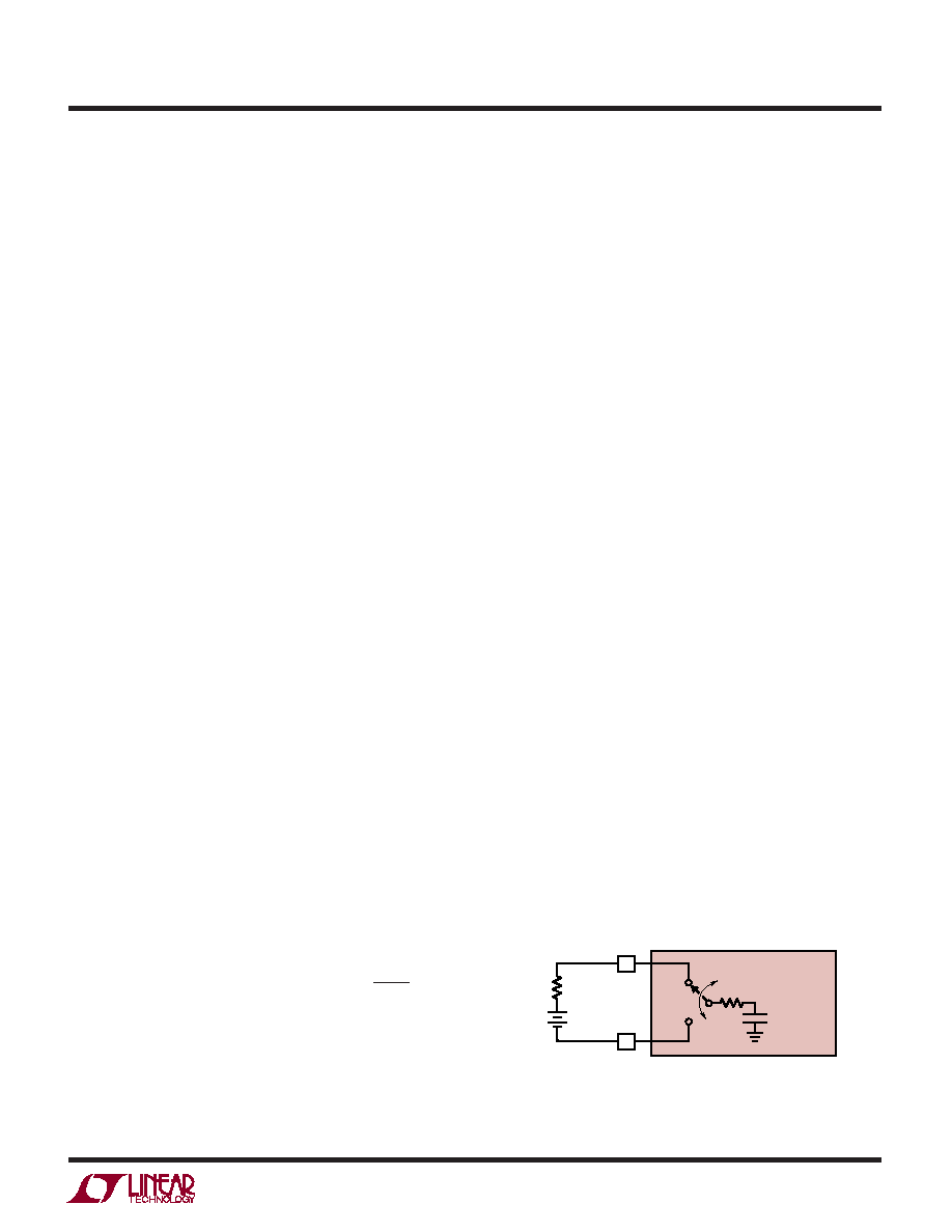
Figure 14. Reference Input Equivalent Circuit
RON
8pF – 40pF
LTC1289
REF+
ROUT
VREF
EVERY 4 ACLK CYCLES
14
13
REF–
LTC1289 AIF14
pins on the package ends (DGND and CH0). Grounding
any unused inputs (especially the end pin, CH0) will also
reduce outside coupling into high source resistances.
4. Sample and Hold
Single-Ended Inputs
The LTC1289 provides a built-in sample and hold (S&H)
function for all signals acquired in the single-ended mode
(COM pin grounded). This sample and hold allows the
LTC1289 to convert rapidly varying signals (see typical
curve of S&H Acquisition Time vs Source Resistance). The
input voltage is sampled during the tSMPL time as shown
in Figure 10. The sampling interval begins after the fourth
MUX address bit is shifted in and continues during the
remainder of the data transfer. On the falling edge of the
final SCLK, the S&H goes into hold mode and the conver-
sion begins. The voltage will be held on either the 8th, 12th
or 16th falling edge of the SCLK depending on the word
length selected.
Differential Inputs
With differential inputs or when the COM pin is not tied to
ground, the A/D no longer converts just a single voltage
but rather the difference between two voltages. In these
cases, the voltage on the selected “+” input is still sampled
and held and therefore may be rapidly time varing just as
in single ended mode. However, the voltage on the se-
lected “–” input must remain constant and be free of noise
and ripple throughout the conversion time. Otherwise, the
differencing operation may not be performed accurately.
The conversion time is 52 ACLK cycles. Therefore, a
change in the “–” input voltage during this interval can
cause conversion errors. For a sinusoidal voltage on the
“–” input this error would be:
VERROR (MAX) = VPEAK × 2 × π × f(“–”) ×
Where f(“–”) is the frequency of the “–” input voltage,
VPEAK is its peak amplitude and fACLK is the frequency of
the ACLK. In most cases VERROR will not be significant. For
U
S
A
O
PPLICATI
WU
U
I FOR ATIO
a 60Hz signal on the “–” input to generate a 1/4LSB error
(150
V) with the converter running at ACLK = 2MHz, its
peak value would have to be 15mV.
5. Reference Inputs
The voltage between the reference inputs of the LTC1289
defines the voltage span of the A/D converter. The refer-
ence inputs will have transient capacitive switching cur-
rents due to the switched capacitor conversion technique
(see Figure 14). During each bit test of the conversion
(every 4 ACLK cycles), a capacitive current spike will be
generated on the reference pins by the A/D. These current
spikes settle quickly and do not cause a problem. How-
ever, if slow settling circuitry is used to drive the reference
inputs, care must be taken to insure that transients caused
by these current spikes settle completely during each bit
test of the conversion.
When driving the reference inputs, two things should be
kept in mind:
1. Transients on the reference inputs caused by the
capacitive switching currents must settle completely
during each bit test (each 4 ACLK cycles). Figures 15
and 16 show examples of both adequate and poor
settling. Using a slower ACLK will allow more time for
the reference to settle. However, even at the maximum
ACLK rate of 2MHz most references and op amps can
be made to settle within the 2
s bit time. For example
an LT1019 used in the shunt mode with a 10
F bypass
capacitor will settle adequately. To minimize power an
LT1004-2.5 can be used with a 10
F bypass capacitor.
For lower value references the LT1004-1.2 with a 1
F
bypass capacitor can be used.
52
fACLK
相关PDF资料 |
PDF描述 |
|---|---|
| LTC1287BCN8 | IC DATA ACQ SYS 12BIT 3V 8-DIP |
| V110A5M200BF | CONVERTER MOD DC/DC 5V 200W |
| LTC1292BIN8#PBF | IC DATA ACQ SYSTEM 12BIT 8-DIP |
| LTC1292BIN8 | IC DATA ACQ SYSTEM 12BIT 8-DIP |
| AD7891APZ-2REEL | IC DAS 12BIT 8CH 44-PLCC |
相关代理商/技术参数 |
参数描述 |
|---|---|
| LTC1289CCSW#PBF | 功能描述:IC DATA ACQ SYS 12BIT 3V 20-SOIC RoHS:是 类别:集成电路 (IC) >> 数据采集 - ADCs/DAC - 专用型 系列:- 产品培训模块:Lead (SnPb) Finish for COTS Obsolescence Mitigation Program 标准包装:50 系列:- 类型:数据采集系统(DAS) 分辨率(位):16 b 采样率(每秒):21.94k 数据接口:MICROWIRE?,QSPI?,串行,SPI? 电压电源:模拟和数字 电源电压:1.8 V ~ 3.6 V 工作温度:-40°C ~ 85°C 安装类型:表面贴装 封装/外壳:40-WFQFN 裸露焊盘 供应商设备封装:40-TQFN-EP(6x6) 包装:托盘 |
| LTC1289CCSW#TR | 功能描述:IC DATA ACQ SYS 12BIT 3V 20SOIC RoHS:否 类别:集成电路 (IC) >> 数据采集 - ADCs/DAC - 专用型 系列:- 产品培训模块:Lead (SnPb) Finish for COTS Obsolescence Mitigation Program 标准包装:50 系列:- 类型:数据采集系统(DAS) 分辨率(位):16 b 采样率(每秒):21.94k 数据接口:MICROWIRE?,QSPI?,串行,SPI? 电压电源:模拟和数字 电源电压:1.8 V ~ 3.6 V 工作温度:-40°C ~ 85°C 安装类型:表面贴装 封装/外壳:40-WFQFN 裸露焊盘 供应商设备封装:40-TQFN-EP(6x6) 包装:托盘 |
| LTC1289CCSW#TRPBF | 功能描述:IC DATA ACQ SYS 12BIT 3V 20-SOIC RoHS:是 类别:集成电路 (IC) >> 数据采集 - ADCs/DAC - 专用型 系列:- 产品培训模块:Lead (SnPb) Finish for COTS Obsolescence Mitigation Program 标准包装:50 系列:- 类型:数据采集系统(DAS) 分辨率(位):16 b 采样率(每秒):21.94k 数据接口:MICROWIRE?,QSPI?,串行,SPI? 电压电源:模拟和数字 电源电压:1.8 V ~ 3.6 V 工作温度:-40°C ~ 85°C 安装类型:表面贴装 封装/外壳:40-WFQFN 裸露焊盘 供应商设备封装:40-TQFN-EP(6x6) 包装:托盘 |
| LTC1290BCJ | 制造商:Linear Technology 功能描述:ADC Single SAR 50ksps 12-bit Serial 20-Pin CDIP |
| LTC1290BCN | 功能描述:IC DATA ACQ SYS 12BIT 20-DIP RoHS:否 类别:集成电路 (IC) >> 数据采集 - ADCs/DAC - 专用型 系列:- 产品培训模块:Lead (SnPb) Finish for COTS Obsolescence Mitigation Program 标准包装:50 系列:- 类型:数据采集系统(DAS) 分辨率(位):16 b 采样率(每秒):21.94k 数据接口:MICROWIRE?,QSPI?,串行,SPI? 电压电源:模拟和数字 电源电压:1.8 V ~ 3.6 V 工作温度:-40°C ~ 85°C 安装类型:表面贴装 封装/外壳:40-WFQFN 裸露焊盘 供应商设备封装:40-TQFN-EP(6x6) 包装:托盘 |
发布紧急采购,3分钟左右您将得到回复。