参数资料
| 型号: | LTC1289CCSW |
| 厂商: | Linear Technology |
| 文件页数: | 26/28页 |
| 文件大小: | 0K |
| 描述: | IC DATA ACQ SYS 12BIT 3V 20-SOIC |
| 标准包装: | 38 |
| 类型: | 数据采集系统(DAS) |
| 分辨率(位): | 12 b |
| 采样率(每秒): | 25k |
| 数据接口: | 串行,并联 |
| 电压电源: | 双 ± |
| 电源电压: | ±3.3V |
| 工作温度: | 0°C ~ 70°C |
| 安装类型: | 表面贴装 |
| 封装/外壳: | 20-SOIC(0.295",7.50mm 宽) |
| 供应商设备封装: | 20-SOIC |
| 包装: | 管件 |
| 其它名称: | LTC1289CCS |
第1页第2页第3页第4页第5页第6页第7页第8页第9页第10页第11页第12页第13页第14页第15页第16页第17页第18页第19页第20页第21页第22页第23页第24页第25页当前第26页第27页第28页
7
LTC1289
1289fb
PI FU CTIO S
U
UU
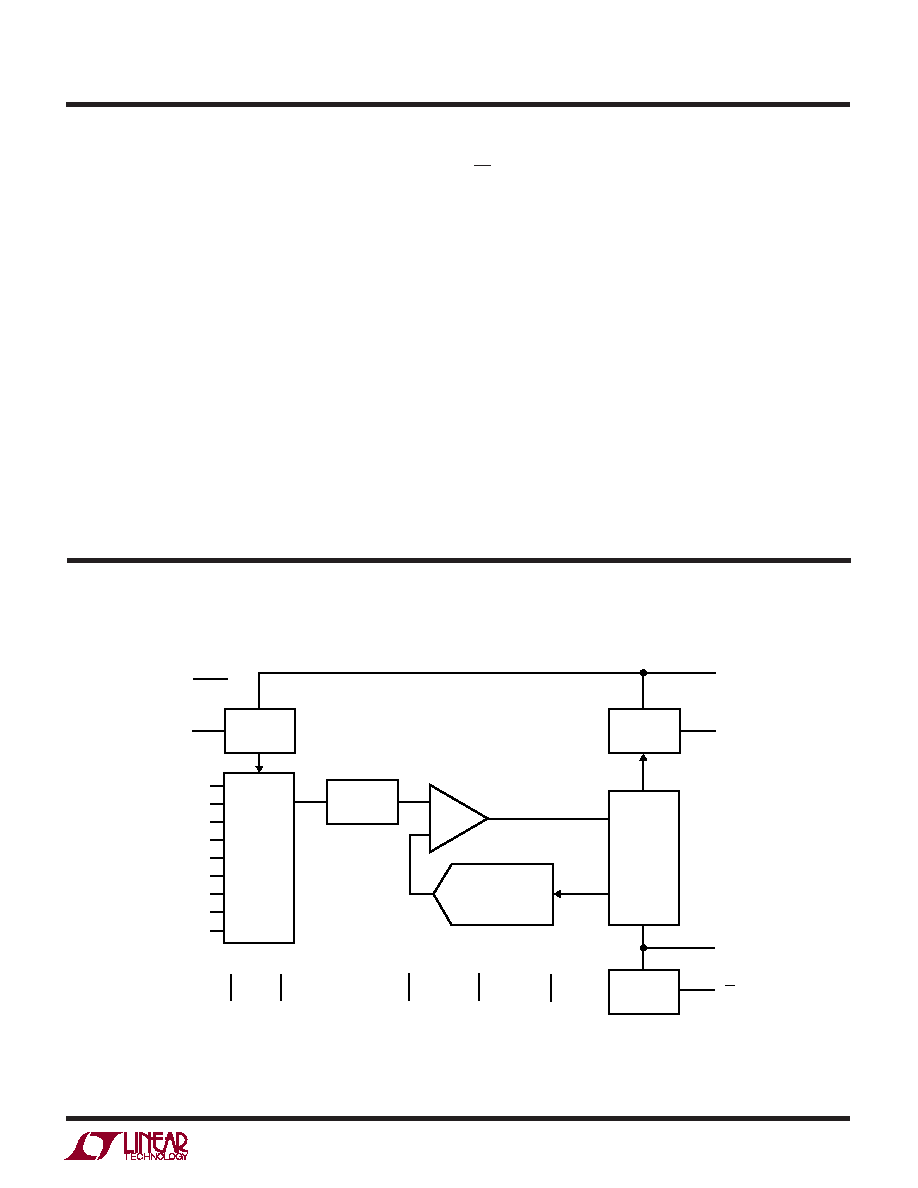
BLOCK DIAGRAM
INPUT
SHIFT
REGISTER
SAMPLE
AND
HOLD
12-BIT
CAPACITIVE
DAC
VCC
20
ANALOG
INPUT MUX
1
2
3
4
5
6
7
8
9
CH0
CH1
CH2
CH3
CH4
CH5
CH6
CH7
COM
DOUT
16
SCLK
18
CONTROL
AND
TIMING
15
CS
LTC1289 BD
17
REF+
14
DGND
10
AGND
11
V–
12
REF–
13
COMP
OUTPUT
SHIFT
REGISTER
DIN
19
ACLK
12-BIT
SAR
CH0 – CH7 (Pins 1 – 8): Analog Inputs. The analog in-
puts must be free of noise with respect to AGND.
COM (Pin 9): Common. The common pin defines the zero
reference point for all single-ended inputs. It must be free
of noise and is usually tied to the analog ground plane.
DGND (Pin 10):Digital Ground. This is the ground for the
internal logic. Tie to the ground plane.
AGND (Pin 11): Analog Ground. AGND should be tied di-
rectly to the analog ground plane.
V– (Pin 12): Negative Supply. Tie V– to the most negative
potential in the circuit. (Ground in single supply applica-
tions.)
REF–, REF+ (Pins 13,14) Reference Inputs. The reference
inputs must be kept free of noise with respect to AGND.
CS (Pin 15): Chip Select Input. A logic low on this input
enables data transfer.
DOUT (Pin 16): Digital Data Output. The A/D conversion
result is shifted out of this output.
DIN (Pin 17): Digital Input. The A/D configuration word is
shifted into this input.
SCLK (Pin 18): Shift Clock. This clock synchronizes the
serial data transfer.
ACLK (Pin 19): A/D Conversion Clock. This clock con-
trols the A/D conversion process.
VCC (Pin 20): Positive Supply. This supply must be kept
free of noise and ripple by bypassing directly to the analog
ground plane.
相关PDF资料 |
PDF描述 |
|---|---|
| LTC1287BCN8 | IC DATA ACQ SYS 12BIT 3V 8-DIP |
| V110A5M200BF | CONVERTER MOD DC/DC 5V 200W |
| LTC1292BIN8#PBF | IC DATA ACQ SYSTEM 12BIT 8-DIP |
| LTC1292BIN8 | IC DATA ACQ SYSTEM 12BIT 8-DIP |
| AD7891APZ-2REEL | IC DAS 12BIT 8CH 44-PLCC |
相关代理商/技术参数 |
参数描述 |
|---|---|
| LTC1289CCSW#PBF | 功能描述:IC DATA ACQ SYS 12BIT 3V 20-SOIC RoHS:是 类别:集成电路 (IC) >> 数据采集 - ADCs/DAC - 专用型 系列:- 产品培训模块:Lead (SnPb) Finish for COTS Obsolescence Mitigation Program 标准包装:50 系列:- 类型:数据采集系统(DAS) 分辨率(位):16 b 采样率(每秒):21.94k 数据接口:MICROWIRE?,QSPI?,串行,SPI? 电压电源:模拟和数字 电源电压:1.8 V ~ 3.6 V 工作温度:-40°C ~ 85°C 安装类型:表面贴装 封装/外壳:40-WFQFN 裸露焊盘 供应商设备封装:40-TQFN-EP(6x6) 包装:托盘 |
| LTC1289CCSW#TR | 功能描述:IC DATA ACQ SYS 12BIT 3V 20SOIC RoHS:否 类别:集成电路 (IC) >> 数据采集 - ADCs/DAC - 专用型 系列:- 产品培训模块:Lead (SnPb) Finish for COTS Obsolescence Mitigation Program 标准包装:50 系列:- 类型:数据采集系统(DAS) 分辨率(位):16 b 采样率(每秒):21.94k 数据接口:MICROWIRE?,QSPI?,串行,SPI? 电压电源:模拟和数字 电源电压:1.8 V ~ 3.6 V 工作温度:-40°C ~ 85°C 安装类型:表面贴装 封装/外壳:40-WFQFN 裸露焊盘 供应商设备封装:40-TQFN-EP(6x6) 包装:托盘 |
| LTC1289CCSW#TRPBF | 功能描述:IC DATA ACQ SYS 12BIT 3V 20-SOIC RoHS:是 类别:集成电路 (IC) >> 数据采集 - ADCs/DAC - 专用型 系列:- 产品培训模块:Lead (SnPb) Finish for COTS Obsolescence Mitigation Program 标准包装:50 系列:- 类型:数据采集系统(DAS) 分辨率(位):16 b 采样率(每秒):21.94k 数据接口:MICROWIRE?,QSPI?,串行,SPI? 电压电源:模拟和数字 电源电压:1.8 V ~ 3.6 V 工作温度:-40°C ~ 85°C 安装类型:表面贴装 封装/外壳:40-WFQFN 裸露焊盘 供应商设备封装:40-TQFN-EP(6x6) 包装:托盘 |
| LTC1290BCJ | 制造商:Linear Technology 功能描述:ADC Single SAR 50ksps 12-bit Serial 20-Pin CDIP |
| LTC1290BCN | 功能描述:IC DATA ACQ SYS 12BIT 20-DIP RoHS:否 类别:集成电路 (IC) >> 数据采集 - ADCs/DAC - 专用型 系列:- 产品培训模块:Lead (SnPb) Finish for COTS Obsolescence Mitigation Program 标准包装:50 系列:- 类型:数据采集系统(DAS) 分辨率(位):16 b 采样率(每秒):21.94k 数据接口:MICROWIRE?,QSPI?,串行,SPI? 电压电源:模拟和数字 电源电压:1.8 V ~ 3.6 V 工作温度:-40°C ~ 85°C 安装类型:表面贴装 封装/外壳:40-WFQFN 裸露焊盘 供应商设备封装:40-TQFN-EP(6x6) 包装:托盘 |
发布紧急采购,3分钟左右您将得到回复。