参数资料
| 型号: | LTC1290BISW#PBF |
| 厂商: | Linear Technology |
| 文件页数: | 14/32页 |
| 文件大小: | 0K |
| 描述: | IC DATA ACQ SYS 12BIT 20-SOIC |
| 标准包装: | 38 |
| 类型: | 数据采集系统(DAS),ADC |
| 分辨率(位): | 12 b |
| 采样率(每秒): | 50k |
| 数据接口: | 串行,并联 |
| 电压电源: | 双 ± |
| 电源电压: | ±5 V,5 V |
| 工作温度: | -40°C ~ 85°C |
| 安装类型: | 表面贴装 |
| 封装/外壳: | 20-SOIC(0.295",7.50mm 宽) |
| 供应商设备封装: | 20-SOIC |
| 包装: | 管件 |
第1页第2页第3页第4页第5页第6页第7页第8页第9页第10页第11页第12页第13页当前第14页第15页第16页第17页第18页第19页第20页第21页第22页第23页第24页第25页第26页第27页第28页第29页第30页第31页第32页
21
LTC1290
1290fe
U
S
A
O
PPLICATI
WU
U
I FOR ATIO
maximum clock rates (ACLK = 4MHz and SCLK = 2MHz).
Figures 11 and 12 show examples of adequate and poor
op amp settling.
HORIZONTAL: 500ns/DIV
Figure 11. Adequate Settling of Op Amps Driving Analog Input
VERTICAL:
5mV/DIV
HORIZONTAL: 20
s/DIV
Figure 12. Poor Op Amp Settling Can Cause A/D Errors
VERTICAL:
5mV/DIV
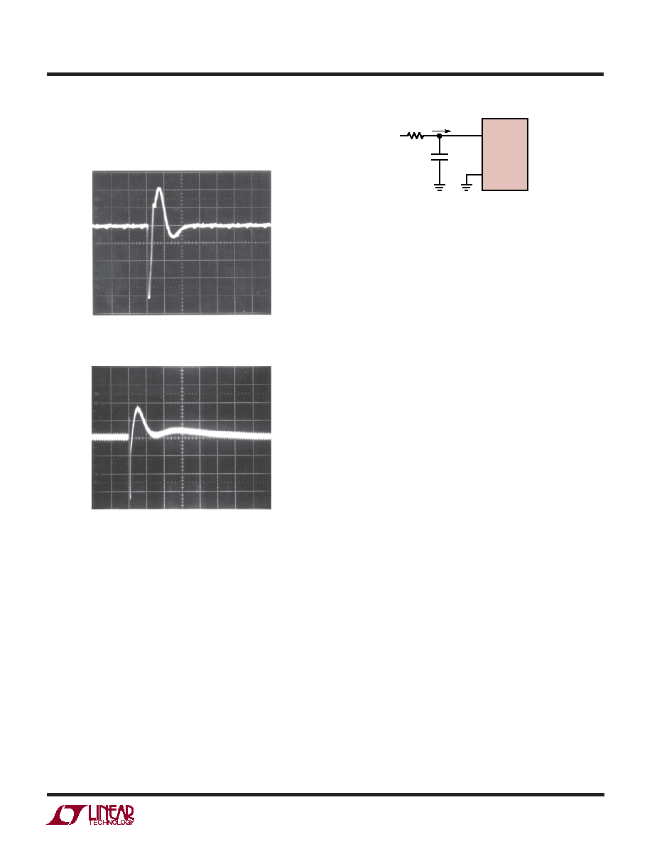
RC Input Filtering
It is possible to filter the inputs with an RC network as shown
in Figure 13. For large values of CF (e.g., 1F), the capacitive
input switching currents are averaged into a net DC current.
Therefore, a filter should be chosen with a small resistor and
large capacitor to prevent DC drops across the resistor. The
magnitude of the DC current is approximately IDC =
(100pF)(VIN/tCYC) and is roughly proportional to VIN. When
running at the minimum cycle time of 20
s, the input
current equals 25
A at VIN = 5V. In this case, a filter resistor
of 5
will cause 0.1LSB of full-scale error. If a larger filter
resistor must be used, errors can be eliminated by increas-
ing the cycle time as shown in the typical curve of Maximum
Filter Resistor vs Cycle Time.
Figure 13. RC Input Filtering
RFILTER
VIN
CFILTER
LTC1290 F13
LTC1290
"+"
"–"
IDC
Input Leakage Current
Input leakage currents can also create errors if the source
resistance gets too large. For instance, the maximum input
leakage specification of 1
A (at 125°C) flowing through a
source resistance of 1k
will cause a voltage drop of 1mV
or 0.8LSB. This error will be much reduced at lower
temperatures because leakage drops rapidly (see the
typical curve of Input Channel Leakage Current vs Tem-
perature).
Noise Coupling Into Inputs
High source resistance input signals (>500
) are more
sensitive to coupling from external sources. It is prefer-
able to use channels near the center of the package (i.e.,
CH2 to CH7) for signals which have the highest output
resistance because they are essentially shielded by the
pins on the package ends (DGND and CH0). Grounding
any unused inputs (especially the end pin, CH0) will also
reduce outside coupling into high source resistances.
4. Sample-and-Hold
Single-Ended Inputs
The LTC1290 provides a built-in sample-and-hold (S&H)
function for all signals acquired in the single-ended mode
(COM pin grounded). This sample-and-hold allows the
LTC1290 to convert rapidly varying signals (see the typical
curve of S&H Acquisition Time vs Source Resistance). The
input voltage is sampled during the tSMPL time as shown in
Figure 10. The sampling interval begins after the fourth MUX
address bit is shifted in and continues during the remainder
of the data transfer. On the falling edge of the final SCLK, the
S&H goes into hold mode and the conversion begins. The
voltage will be held on either the 8th, 12th or 16th falling edge
of the SCLK depending on the word length selected.
相关PDF资料 |
PDF描述 |
|---|---|
| VE-B3H-IU | CONVERTER MOD DC/DC 52V 200W |
| VI-B5L-MY-S | CONVERTER MOD DC/DC 28V 50W |
| V110A12M300BL2 | CONVERTER MOD DC/DC 12V 300W |
| MS27497T20F39SA | CONN RCPT 39POS WALL MNT W/SCKT |
| V110A12M300BL | CONVERTER MOD DC/DC 12V 300W |
相关代理商/技术参数 |
参数描述 |
|---|---|
| LTC1290CCJ | 制造商:Linear Technology 功能描述: |
| LTC1290CCN | 功能描述:IC DATA ACQ SYS 12BIT 20-DIP RoHS:否 类别:集成电路 (IC) >> 数据采集 - ADCs/DAC - 专用型 系列:- 产品培训模块:Lead (SnPb) Finish for COTS Obsolescence Mitigation Program 标准包装:50 系列:- 类型:数据采集系统(DAS) 分辨率(位):16 b 采样率(每秒):21.94k 数据接口:MICROWIRE?,QSPI?,串行,SPI? 电压电源:模拟和数字 电源电压:1.8 V ~ 3.6 V 工作温度:-40°C ~ 85°C 安装类型:表面贴装 封装/外壳:40-WFQFN 裸露焊盘 供应商设备封装:40-TQFN-EP(6x6) 包装:托盘 |
| LTC1290CCN#PBF | 功能描述:IC DATA ACQ SYS 12BIT 20-DIP RoHS:是 类别:集成电路 (IC) >> 数据采集 - ADCs/DAC - 专用型 系列:- 产品培训模块:Data Converter Basics 标准包装:1 系列:- 类型:电机控制 分辨率(位):12 b 采样率(每秒):1M 数据接口:串行,并联 电压电源:单电源 电源电压:2.7 V ~ 3.6 V,4.5 V ~ 5.5 V 工作温度:-40°C ~ 85°C 安装类型:表面贴装 封装/外壳:100-TQFP 供应商设备封装:100-TQFP(14x14) 包装:剪切带 (CT) 其它名称:296-18373-1 |
| LTC1290CCNPBF | 制造商:Linear Technology 功能描述:ADC SAR 50ksps 12-Bit Serial PDIP20 |
| LTC1290CCSW | 功能描述:IC DATA ACQ SYS 12BIT 20-SOIC RoHS:否 类别:集成电路 (IC) >> 数据采集 - ADCs/DAC - 专用型 系列:- 产品培训模块:Lead (SnPb) Finish for COTS Obsolescence Mitigation Program 标准包装:50 系列:- 类型:数据采集系统(DAS) 分辨率(位):16 b 采样率(每秒):21.94k 数据接口:MICROWIRE?,QSPI?,串行,SPI? 电压电源:模拟和数字 电源电压:1.8 V ~ 3.6 V 工作温度:-40°C ~ 85°C 安装类型:表面贴装 封装/外壳:40-WFQFN 裸露焊盘 供应商设备封装:40-TQFN-EP(6x6) 包装:托盘 |
发布紧急采购,3分钟左右您将得到回复。