参数资料
| 型号: | LTC1290BISW#PBF |
| 厂商: | Linear Technology |
| 文件页数: | 17/32页 |
| 文件大小: | 0K |
| 描述: | IC DATA ACQ SYS 12BIT 20-SOIC |
| 标准包装: | 38 |
| 类型: | 数据采集系统(DAS),ADC |
| 分辨率(位): | 12 b |
| 采样率(每秒): | 50k |
| 数据接口: | 串行,并联 |
| 电压电源: | 双 ± |
| 电源电压: | ±5 V,5 V |
| 工作温度: | -40°C ~ 85°C |
| 安装类型: | 表面贴装 |
| 封装/外壳: | 20-SOIC(0.295",7.50mm 宽) |
| 供应商设备封装: | 20-SOIC |
| 包装: | 管件 |
第1页第2页第3页第4页第5页第6页第7页第8页第9页第10页第11页第12页第13页第14页第15页第16页当前第17页第18页第19页第20页第21页第22页第23页第24页第25页第26页第27页第28页第29页第30页第31页第32页
24
LTC1290
1290fe
U
S
A
O
PPLICATI
WU
U
I FOR ATIO
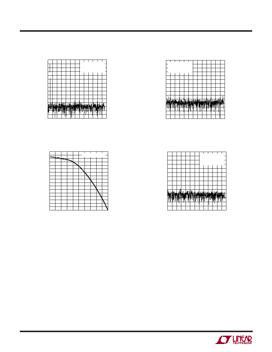
FREQUENCY (kHz)
0
8
12
16
20
424
MAGNITUDE
(dB)
1290 F17a
0
–20
–40
–60
–80
–100
–120
–140
fIN = 1kHz
fSAMPLE = 50.6kHz
SNR = 73.25dB
Figure 17a. LTC1290 FFT Plot
FREQUENCY (kHz)
0
8
12
16
20
424
MAGNITUDE
(dB)
1290 F17b
0
–20
–40
–60
–80
–100
–120
–140
fIN = 25kHz
fSAMPLE = 50.6kHz
SNR = 72.54dB
Figure 17b. LTC1290 FFT Plot
FREQUENCY (kHz)
0
EFFECTIVE
NUMBER
OF
BITS
80
1290 F18
20
40
100
12
11.6
11.2
10.8
10.4
10
9.6
9.2
8.8
60
fSAMPLE = 50.6kHz
Figure 18. LTC1290 ENOB vs Input Frequency
Figure 19. LTC1290 FFT Plot
FREQUENCY (kHz)
0
8
12
16
20
424
MAGNITUDE
(dB)
1290 F19
0
–20
–40
–60
–80
–100
–120
fIN1 = 5.1kHz
fIN2 = 5.6kHz
fSAMPLE = 50.6kHz
8. Overvoltage Protection
Applying signals to the analog MUX that exceed the
positive or negative supply of the device will degrade the
accuracy of the A/D and possibly damage the device. For
example this condition would occur if a signal is applied to
the analog MUX before power is applied to the LTC1290.
Another example is the input source is operating from
different supplies of larger value than the LTC1290. These
conditions should be prevented either with proper supply
sequencing or by use of external circuitry to clamp or
current limit the input source. As shown in Figure 20, a 1k
resistor is enough to stand off
±15V (15mA for one only
channel). If more than one channel exceeds the supplies
then the following guidelines can be used. Limit the
current to 7mA per channel and 28mA for all channels.
This means four channels can handle 7mA of input current
each. Reducing the ACLK and SCLK frequencies from the
maximum of 4MHz and 2MHz, respectively, (see Typical
Performance Characteristics curves Maximum ACLK Fre-
quency vs Source Resistance and Sample-and-Hold
Acquisition Time vs Source Resistance) allows the use of
larger current limiting resistors. Use 1N4148 diode clamps
from the MUX inputs to VCC and V – if the value of the series
resistor will not allow the maximum clock speeds to be
used or if an unknown source is used to drive the LTC1290
MUX inputs.
相关PDF资料 |
PDF描述 |
|---|---|
| VE-B3H-IU | CONVERTER MOD DC/DC 52V 200W |
| VI-B5L-MY-S | CONVERTER MOD DC/DC 28V 50W |
| V110A12M300BL2 | CONVERTER MOD DC/DC 12V 300W |
| MS27497T20F39SA | CONN RCPT 39POS WALL MNT W/SCKT |
| V110A12M300BL | CONVERTER MOD DC/DC 12V 300W |
相关代理商/技术参数 |
参数描述 |
|---|---|
| LTC1290CCJ | 制造商:Linear Technology 功能描述: |
| LTC1290CCN | 功能描述:IC DATA ACQ SYS 12BIT 20-DIP RoHS:否 类别:集成电路 (IC) >> 数据采集 - ADCs/DAC - 专用型 系列:- 产品培训模块:Lead (SnPb) Finish for COTS Obsolescence Mitigation Program 标准包装:50 系列:- 类型:数据采集系统(DAS) 分辨率(位):16 b 采样率(每秒):21.94k 数据接口:MICROWIRE?,QSPI?,串行,SPI? 电压电源:模拟和数字 电源电压:1.8 V ~ 3.6 V 工作温度:-40°C ~ 85°C 安装类型:表面贴装 封装/外壳:40-WFQFN 裸露焊盘 供应商设备封装:40-TQFN-EP(6x6) 包装:托盘 |
| LTC1290CCN#PBF | 功能描述:IC DATA ACQ SYS 12BIT 20-DIP RoHS:是 类别:集成电路 (IC) >> 数据采集 - ADCs/DAC - 专用型 系列:- 产品培训模块:Data Converter Basics 标准包装:1 系列:- 类型:电机控制 分辨率(位):12 b 采样率(每秒):1M 数据接口:串行,并联 电压电源:单电源 电源电压:2.7 V ~ 3.6 V,4.5 V ~ 5.5 V 工作温度:-40°C ~ 85°C 安装类型:表面贴装 封装/外壳:100-TQFP 供应商设备封装:100-TQFP(14x14) 包装:剪切带 (CT) 其它名称:296-18373-1 |
| LTC1290CCNPBF | 制造商:Linear Technology 功能描述:ADC SAR 50ksps 12-Bit Serial PDIP20 |
| LTC1290CCSW | 功能描述:IC DATA ACQ SYS 12BIT 20-SOIC RoHS:否 类别:集成电路 (IC) >> 数据采集 - ADCs/DAC - 专用型 系列:- 产品培训模块:Lead (SnPb) Finish for COTS Obsolescence Mitigation Program 标准包装:50 系列:- 类型:数据采集系统(DAS) 分辨率(位):16 b 采样率(每秒):21.94k 数据接口:MICROWIRE?,QSPI?,串行,SPI? 电压电源:模拟和数字 电源电压:1.8 V ~ 3.6 V 工作温度:-40°C ~ 85°C 安装类型:表面贴装 封装/外壳:40-WFQFN 裸露焊盘 供应商设备封装:40-TQFN-EP(6x6) 包装:托盘 |
发布紧急采购,3分钟左右您将得到回复。