参数资料
| 型号: | LTC1290DCSW#PBF |
| 厂商: | Linear Technology |
| 文件页数: | 15/32页 |
| 文件大小: | 0K |
| 描述: | IC DATA ACQ SYS 12BIT 20-SOIC |
| 标准包装: | 38 |
| 类型: | 数据采集系统(DAS),ADC |
| 分辨率(位): | 12 b |
| 采样率(每秒): | 50k |
| 数据接口: | 串行,并联 |
| 电压电源: | 双 ± |
| 电源电压: | ±5 V,5 V |
| 工作温度: | 0°C ~ 70°C |
| 安装类型: | 表面贴装 |
| 封装/外壳: | 20-SOIC(0.295",7.50mm 宽) |
| 供应商设备封装: | 20-SOIC |
| 包装: | 管件 |
| 产品目录页面: | 1346 (CN2011-ZH PDF) |
第1页第2页第3页第4页第5页第6页第7页第8页第9页第10页第11页第12页第13页第14页当前第15页第16页第17页第18页第19页第20页第21页第22页第23页第24页第25页第26页第27页第28页第29页第30页第31页第32页
22
LTC1290
1290fe
U
S
A
O
PPLICATI
WU
U
I FOR ATIO
Differential Inputs
With differential inputs or when the COM pin is not tied to
ground, the A/D no longer converts just a single voltage but
rather the difference between two voltages. In these cases,
the voltage on the selected “+” input is still sampled and held
and therefore may be rapidly time varying just as in single-
ended mode. However, the voltage on the selected “–” input
must remain constant and be free of noise and ripple
throughout the conversion time. Otherwise, the differencing
operation may not be performed accurately. The conversion
time is 52 ACLK cycles. Therefore, a change in the “–” input
voltage during this interval can cause conversion errors.
For a sinusoidal voltage on the “–” input this error would be:
VERROR (MAX) = (VPEAK)(2π)[ f(“–”)](52/fACLK)
Where f(“–”) is the frequency of the “–” input voltage,
VPEAK is its peak amplitude and fACLK is the frequency of
the ACLK. In most cases VERROR will not be significant. For
a 60Hz signal on the “–” input to generate a 0.25LSB error
(300
V) with the converter running at ACLK = 4MHz, its
peak value would have to be 61mV.
5. Reference Inputs
The voltage between the reference inputs of the LTC1290
defines the voltage span of the A/D converter. The refer-
ence inputs will have transient capacitive switching cur-
rents due to the switched capacitor conversion technique
(see Figure 14). During each bit test of the conversion
(every 4 ACLK cycles), a capacitive current spike will be
generated on the reference pins by the A/D. These current
spikes settle quickly and do not cause a problem. How-
ever, if slow settling circuitry is used to drive the reference
inputs, care must be taken to insure that transients caused
by these current spikes settle completely during each bit
test of the conversion.
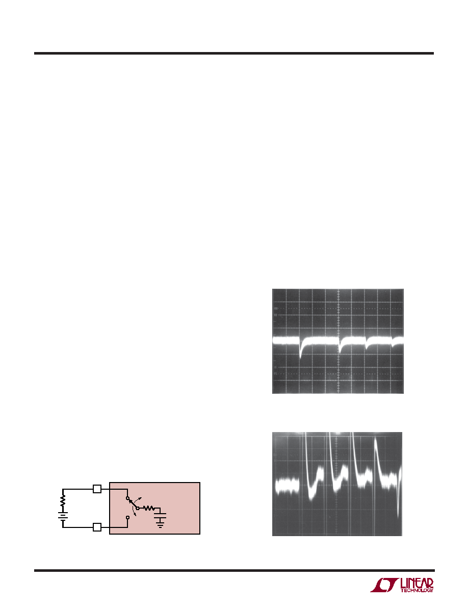
Figure 14. Reference Input Equivalent Circuit
RON
8pF TO 40pF
LTC1290
REF+
ROUT
VREF
EVERY 4 ACLK CYCLES
14
13
REF–
LTC 1290 F14
When driving the reference inputs, two things should be
kept in mind:
1. Transients on the reference inputs caused by the
capacitive switching currents must settle completely
during each bit test (each 4 ACLK cycles). Figures 15
and 16 show examples of both adequate and poor
settling. Using a slower ACLK will allow more time for
the reference to settle. However, even at the maximum
ACLK rate of 4MHz most references and op amps can
be made to settle within the 1
s bit time. For example
the LT1236 will settle adequately.
2. It is recommended that REF– input be tied directly to
the analog ground plane. If REF– is biased at a voltage
other than ground, the voltage must not change during
a conversion cycle. This voltage must also be free of
noise and ripple with respect to analog ground.
Figure 16. Poor Reference Settling Can Cause A/D Errors
HORIZONTAL: 1
s/DIV
VERTICAL:
0.5mV/DIV
Figure 15. Adequate Reference Settling
HORIZONTAL: 1
s/DIV
VERTICAL:
0.5mV/DIV
相关PDF资料 |
PDF描述 |
|---|---|
| VE-B5T-MY-S | CONVERTER MOD DC/DC 6.5V 50W |
| D38999/26JH55JB | CONN PLUG 55POS STRAIGHT W/SCKT |
| VE-B5R-MY-S | CONVERTER MOD DC/DC 7.5V 50W |
| VE-B5P-MY-S | CONVERTER MOD DC/DC 13.8V 50W |
| D38999/26WJ90SN | CONN PLUG 46POS STRAIGHT W/SCKT |
相关代理商/技术参数 |
参数描述 |
|---|---|
| LTC1290DIN | 功能描述:IC DATA ACQ SYS 12BIT 20-DIP RoHS:否 类别:集成电路 (IC) >> 数据采集 - ADCs/DAC - 专用型 系列:- 产品培训模块:Lead (SnPb) Finish for COTS Obsolescence Mitigation Program 标准包装:50 系列:- 类型:数据采集系统(DAS) 分辨率(位):16 b 采样率(每秒):21.94k 数据接口:MICROWIRE?,QSPI?,串行,SPI? 电压电源:模拟和数字 电源电压:1.8 V ~ 3.6 V 工作温度:-40°C ~ 85°C 安装类型:表面贴装 封装/外壳:40-WFQFN 裸露焊盘 供应商设备封装:40-TQFN-EP(6x6) 包装:托盘 |
| LTC1290DIN#PBF | 功能描述:IC DATA ACQ SYS 12BIT 20-DIP RoHS:是 类别:集成电路 (IC) >> 数据采集 - ADCs/DAC - 专用型 系列:- 产品培训模块:Lead (SnPb) Finish for COTS Obsolescence Mitigation Program 标准包装:50 系列:- 类型:数据采集系统(DAS) 分辨率(位):16 b 采样率(每秒):21.94k 数据接口:MICROWIRE?,QSPI?,串行,SPI? 电压电源:模拟和数字 电源电压:1.8 V ~ 3.6 V 工作温度:-40°C ~ 85°C 安装类型:表面贴装 封装/外壳:40-WFQFN 裸露焊盘 供应商设备封装:40-TQFN-EP(6x6) 包装:托盘 |
| LTC1290DISW | 功能描述:IC DATA ACQ SYS 12BIT 20-SOIC RoHS:否 类别:集成电路 (IC) >> 数据采集 - ADCs/DAC - 专用型 系列:- 产品培训模块:Lead (SnPb) Finish for COTS Obsolescence Mitigation Program 标准包装:50 系列:- 类型:数据采集系统(DAS) 分辨率(位):16 b 采样率(每秒):21.94k 数据接口:MICROWIRE?,QSPI?,串行,SPI? 电压电源:模拟和数字 电源电压:1.8 V ~ 3.6 V 工作温度:-40°C ~ 85°C 安装类型:表面贴装 封装/外壳:40-WFQFN 裸露焊盘 供应商设备封装:40-TQFN-EP(6x6) 包装:托盘 |
| LTC1290DISW#PBF | 功能描述:IC DATA ACQ SYS 12BIT 20-SOIC RoHS:是 类别:集成电路 (IC) >> 数据采集 - ADCs/DAC - 专用型 系列:- 产品培训模块:Lead (SnPb) Finish for COTS Obsolescence Mitigation Program 标准包装:50 系列:- 类型:数据采集系统(DAS) 分辨率(位):16 b 采样率(每秒):21.94k 数据接口:MICROWIRE?,QSPI?,串行,SPI? 电压电源:模拟和数字 电源电压:1.8 V ~ 3.6 V 工作温度:-40°C ~ 85°C 安装类型:表面贴装 封装/外壳:40-WFQFN 裸露焊盘 供应商设备封装:40-TQFN-EP(6x6) 包装:托盘 |
| LTC1290DISW#TR | 功能描述:IC DATA ACQ SYS 12BIT 5V 20SOIC RoHS:否 类别:集成电路 (IC) >> 数据采集 - ADCs/DAC - 专用型 系列:- 产品培训模块:Lead (SnPb) Finish for COTS Obsolescence Mitigation Program 标准包装:50 系列:- 类型:数据采集系统(DAS) 分辨率(位):16 b 采样率(每秒):21.94k 数据接口:MICROWIRE?,QSPI?,串行,SPI? 电压电源:模拟和数字 电源电压:1.8 V ~ 3.6 V 工作温度:-40°C ~ 85°C 安装类型:表面贴装 封装/外壳:40-WFQFN 裸露焊盘 供应商设备封装:40-TQFN-EP(6x6) 包装:托盘 |
发布紧急采购,3分钟左右您将得到回复。