参数资料
| 型号: | LTC1290DCSW#PBF |
| 厂商: | Linear Technology |
| 文件页数: | 18/32页 |
| 文件大小: | 0K |
| 描述: | IC DATA ACQ SYS 12BIT 20-SOIC |
| 标准包装: | 38 |
| 类型: | 数据采集系统(DAS),ADC |
| 分辨率(位): | 12 b |
| 采样率(每秒): | 50k |
| 数据接口: | 串行,并联 |
| 电压电源: | 双 ± |
| 电源电压: | ±5 V,5 V |
| 工作温度: | 0°C ~ 70°C |
| 安装类型: | 表面贴装 |
| 封装/外壳: | 20-SOIC(0.295",7.50mm 宽) |
| 供应商设备封装: | 20-SOIC |
| 包装: | 管件 |
| 产品目录页面: | 1346 (CN2011-ZH PDF) |
第1页第2页第3页第4页第5页第6页第7页第8页第9页第10页第11页第12页第13页第14页第15页第16页第17页当前第18页第19页第20页第21页第22页第23页第24页第25页第26页第27页第28页第29页第30页第31页第32页
25
LTC1290
1290fe
U
S
A
O
PPLICATI
WU
U
I FOR ATIO
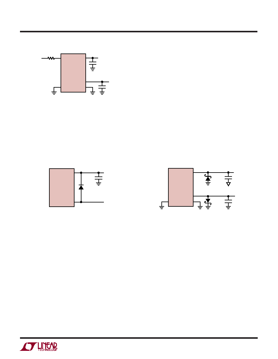
How the various power supplies to the LTC1290 are
applied can also lead to overvoltage conditions. For single
supply operation (i.e., unipolar mode), if VCC and REF+ are
not tied together, then VCC should be turned on first, then
REF+. If this sequence cannot be met, connecting a diode
from REF+ to VCC is recommended (see Figure 21).
For dual supplies (bipolar mode) placing two Schottky
diodes from VCC and V– to ground (Figure 23) will prevent
power supply reversal from occurring when an input
source is applied to the analog MUX before power is
applied to the device. Power supply reversal occurs, for
example, if the input is pulled below V– then VCC will pull
a diode drop below ground which could cause the device
not to power up properly. Likewise, if the input is pulled
above VCC then V– will be pulled a diode drop above
ground. If no inputs are present on the MUX, the Schottky
diodes are not required if V– is applied first, then VCC.
Because a unique input protection structure is used on the
digital input pins, the signal levels on these pins can
exceed the device VCC without damaging the device.
5V
1290 F21
REF+
VCC
LTC1290
22
F
1N4148
VREF
14
20
5V
1290 F22
DGND
V –
AGND
VCC
LTC1290
–5V
0.1
F
22
F
1N5817
Figure 21
Figure 22. Power Supply Reversal
Figure 20. Overvoltage Protection for MUX
5V
1290 F20
DGND
V–
AGND
VCC
1k
LTC1290
CH0
VIN
–5V
0.1
F
22
F
相关PDF资料 |
PDF描述 |
|---|---|
| VE-B5T-MY-S | CONVERTER MOD DC/DC 6.5V 50W |
| D38999/26JH55JB | CONN PLUG 55POS STRAIGHT W/SCKT |
| VE-B5R-MY-S | CONVERTER MOD DC/DC 7.5V 50W |
| VE-B5P-MY-S | CONVERTER MOD DC/DC 13.8V 50W |
| D38999/26WJ90SN | CONN PLUG 46POS STRAIGHT W/SCKT |
相关代理商/技术参数 |
参数描述 |
|---|---|
| LTC1290DIN | 功能描述:IC DATA ACQ SYS 12BIT 20-DIP RoHS:否 类别:集成电路 (IC) >> 数据采集 - ADCs/DAC - 专用型 系列:- 产品培训模块:Lead (SnPb) Finish for COTS Obsolescence Mitigation Program 标准包装:50 系列:- 类型:数据采集系统(DAS) 分辨率(位):16 b 采样率(每秒):21.94k 数据接口:MICROWIRE?,QSPI?,串行,SPI? 电压电源:模拟和数字 电源电压:1.8 V ~ 3.6 V 工作温度:-40°C ~ 85°C 安装类型:表面贴装 封装/外壳:40-WFQFN 裸露焊盘 供应商设备封装:40-TQFN-EP(6x6) 包装:托盘 |
| LTC1290DIN#PBF | 功能描述:IC DATA ACQ SYS 12BIT 20-DIP RoHS:是 类别:集成电路 (IC) >> 数据采集 - ADCs/DAC - 专用型 系列:- 产品培训模块:Lead (SnPb) Finish for COTS Obsolescence Mitigation Program 标准包装:50 系列:- 类型:数据采集系统(DAS) 分辨率(位):16 b 采样率(每秒):21.94k 数据接口:MICROWIRE?,QSPI?,串行,SPI? 电压电源:模拟和数字 电源电压:1.8 V ~ 3.6 V 工作温度:-40°C ~ 85°C 安装类型:表面贴装 封装/外壳:40-WFQFN 裸露焊盘 供应商设备封装:40-TQFN-EP(6x6) 包装:托盘 |
| LTC1290DISW | 功能描述:IC DATA ACQ SYS 12BIT 20-SOIC RoHS:否 类别:集成电路 (IC) >> 数据采集 - ADCs/DAC - 专用型 系列:- 产品培训模块:Lead (SnPb) Finish for COTS Obsolescence Mitigation Program 标准包装:50 系列:- 类型:数据采集系统(DAS) 分辨率(位):16 b 采样率(每秒):21.94k 数据接口:MICROWIRE?,QSPI?,串行,SPI? 电压电源:模拟和数字 电源电压:1.8 V ~ 3.6 V 工作温度:-40°C ~ 85°C 安装类型:表面贴装 封装/外壳:40-WFQFN 裸露焊盘 供应商设备封装:40-TQFN-EP(6x6) 包装:托盘 |
| LTC1290DISW#PBF | 功能描述:IC DATA ACQ SYS 12BIT 20-SOIC RoHS:是 类别:集成电路 (IC) >> 数据采集 - ADCs/DAC - 专用型 系列:- 产品培训模块:Lead (SnPb) Finish for COTS Obsolescence Mitigation Program 标准包装:50 系列:- 类型:数据采集系统(DAS) 分辨率(位):16 b 采样率(每秒):21.94k 数据接口:MICROWIRE?,QSPI?,串行,SPI? 电压电源:模拟和数字 电源电压:1.8 V ~ 3.6 V 工作温度:-40°C ~ 85°C 安装类型:表面贴装 封装/外壳:40-WFQFN 裸露焊盘 供应商设备封装:40-TQFN-EP(6x6) 包装:托盘 |
| LTC1290DISW#TR | 功能描述:IC DATA ACQ SYS 12BIT 5V 20SOIC RoHS:否 类别:集成电路 (IC) >> 数据采集 - ADCs/DAC - 专用型 系列:- 产品培训模块:Lead (SnPb) Finish for COTS Obsolescence Mitigation Program 标准包装:50 系列:- 类型:数据采集系统(DAS) 分辨率(位):16 b 采样率(每秒):21.94k 数据接口:MICROWIRE?,QSPI?,串行,SPI? 电压电源:模拟和数字 电源电压:1.8 V ~ 3.6 V 工作温度:-40°C ~ 85°C 安装类型:表面贴装 封装/外壳:40-WFQFN 裸露焊盘 供应商设备封装:40-TQFN-EP(6x6) 包装:托盘 |
发布紧急采购,3分钟左右您将得到回复。