- 您现在的位置:买卖IC网 > PDF目录39406 > LTC1294BCJ (LINEAR TECHNOLOGY CORP) 8-CH 12-BIT SUCCESSIVE APPROXIMATION ADC, SERIAL ACCESS, CDIP20 PDF资料下载
参数资料
| 型号: | LTC1294BCJ |
| 厂商: | LINEAR TECHNOLOGY CORP |
| 元件分类: | ADC |
| 英文描述: | 8-CH 12-BIT SUCCESSIVE APPROXIMATION ADC, SERIAL ACCESS, CDIP20 |
| 封装: | CERDIP-20 |
| 文件页数: | 11/28页 |
| 文件大小: | 383K |
| 代理商: | LTC1294BCJ |
第1页第2页第3页第4页第5页第6页第7页第8页第9页第10页当前第11页第12页第13页第14页第15页第16页第17页第18页第19页第20页第21页第22页第23页第24页第25页第26页第27页第28页
19
LTC1293/LTC1294/LTC1296
129346fs
U
S
A
O
PPLICATI
WU
U
I FOR ATIO
Source Resistance
The analog inputs of the LTC1293/4/6 look like a 100pF
capacitor (CIN) in series with a 500 resistor (RON). CIN
gets switched between (+) and (–) inputs once during each
conversion cycle. Large external source resistors and
capacitances will slow the settling of the inputs. It is
important that the overall RC time constant is short
enough to allow the analog inputs to settle completely
within the allowed time.
“+” Input Settling
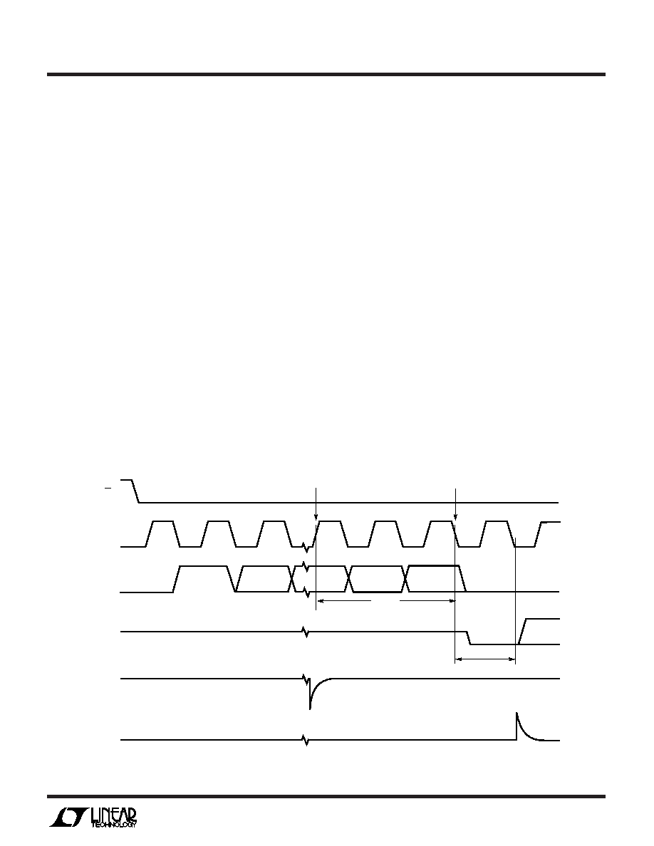
The input capacitor is switched onto the “+” input during
the sample phase (tSMPL, see Figure 8). The sample period
2 1/2 CLK cycles before a conversion starts. The voltage on
the “+” input must settle completely within the sample
period. Minimizing RSOURCE+ and C1 will improve the
settling time. If large “+” input source resistance must be
used, the sample time can be increased by using a slower
CLK frequency. With the minimum possible sample time
of 2.5
s RSOURCE+ < 1.5k
and C1 < 20pF will provide
adequate settling time.
“–” Input Settling
At the end of the sample phase the input capacitor switches
to the “-” input and the conversion starts (see Figure 8).
During the conversion, the “+” input voltage is effectively
“held” by the sample and hold and will not affect the
conversion result. It is critical that the “–” input voltage be
free of noise and settle completely during the first CLK
cycle of the conversion. Minimizing RSOURCE– and C2 will
improve settling time. If large “–” input source resistance
must be used the time can be extended by using a slower
CLK frequency. At the maximum CLK frequency of 1MHz,
RSOURCE– < 250
and C2 < 20pF will provide adequate
settling.
Input Op Amps
When driving the analog inputs with an op amp it is
important that the op amp settles within the allowed time
(see Figure 8). Again the “+” and “–” input sampling times
can be extended as described above to accommodate
slower op amps. Most op amps including the LT1006 and
LT1013 single supply op amps can be made to settle
Figure 8. “+” and “–” Input Settling Windows
DIN
CLK
START
HI-Z
LTC1293 F08
CS
1ST BIT TEST (–) INPUT MUST
SETTLE DURING THIS TIME
tSMPL
(+) INPUT MUST SETTLE DURING THIS TIME
(+) INPUT
(–) INPUT
SGL/
DIFF
MSBF
PS
DOUT
B11
SAMPLE
HOLD
相关PDF资料 |
PDF描述 |
|---|---|
| LTC1294CCJ | 8-CH 12-BIT SUCCESSIVE APPROXIMATION ADC, SERIAL ACCESS, CDIP20 |
| LTC1296BCJ | 8-CH 12-BIT SUCCESSIVE APPROXIMATION ADC, SERIAL ACCESS, CDIP20 |
| LTC1296CCJ | 8-CH 12-BIT SUCCESSIVE APPROXIMATION ADC, SERIAL ACCESS, CDIP20 |
| LTC1294DCJ | 8-CH 12-BIT SUCCESSIVE APPROXIMATION ADC, SERIAL ACCESS, CDIP20 |
| LTC1296DCJ | 8-CH 12-BIT SUCCESSIVE APPROXIMATION ADC, SERIAL ACCESS, CDIP20 |
相关代理商/技术参数 |
参数描述 |
|---|---|
| LTC1294BCN | 功能描述:IC DATA ACQ SYSTEM 12BIT 20-DIP RoHS:否 类别:集成电路 (IC) >> 数据采集 - ADCs/DAC - 专用型 系列:- 产品培训模块:Lead (SnPb) Finish for COTS Obsolescence Mitigation Program 标准包装:50 系列:- 类型:数据采集系统(DAS) 分辨率(位):16 b 采样率(每秒):21.94k 数据接口:MICROWIRE?,QSPI?,串行,SPI? 电压电源:模拟和数字 电源电压:1.8 V ~ 3.6 V 工作温度:-40°C ~ 85°C 安装类型:表面贴装 封装/外壳:40-WFQFN 裸露焊盘 供应商设备封装:40-TQFN-EP(6x6) 包装:托盘 |
| LTC1294BCN#PBF | 功能描述:IC DATA ACQ SYSTEM 12BIT 20-DIP RoHS:是 类别:集成电路 (IC) >> 数据采集 - ADCs/DAC - 专用型 系列:- 产品培训模块:Lead (SnPb) Finish for COTS Obsolescence Mitigation Program 标准包装:50 系列:- 类型:数据采集系统(DAS) 分辨率(位):16 b 采样率(每秒):21.94k 数据接口:MICROWIRE?,QSPI?,串行,SPI? 电压电源:模拟和数字 电源电压:1.8 V ~ 3.6 V 工作温度:-40°C ~ 85°C 安装类型:表面贴装 封装/外壳:40-WFQFN 裸露焊盘 供应商设备封装:40-TQFN-EP(6x6) 包装:托盘 |
| LTC1294BCSW | 功能描述:IC DATA ACQ SYSTEM 12BIT 20-SOIC RoHS:否 类别:集成电路 (IC) >> 数据采集 - ADCs/DAC - 专用型 系列:- 产品培训模块:Lead (SnPb) Finish for COTS Obsolescence Mitigation Program 标准包装:50 系列:- 类型:数据采集系统(DAS) 分辨率(位):16 b 采样率(每秒):21.94k 数据接口:MICROWIRE?,QSPI?,串行,SPI? 电压电源:模拟和数字 电源电压:1.8 V ~ 3.6 V 工作温度:-40°C ~ 85°C 安装类型:表面贴装 封装/外壳:40-WFQFN 裸露焊盘 供应商设备封装:40-TQFN-EP(6x6) 包装:托盘 |
| LTC1294BCSW#PBF | 功能描述:IC DATA ACQ SYSTEM 12BIT 20-SOIC RoHS:是 类别:集成电路 (IC) >> 数据采集 - ADCs/DAC - 专用型 系列:- 产品培训模块:Lead (SnPb) Finish for COTS Obsolescence Mitigation Program 标准包装:50 系列:- 类型:数据采集系统(DAS) 分辨率(位):16 b 采样率(每秒):21.94k 数据接口:MICROWIRE?,QSPI?,串行,SPI? 电压电源:模拟和数字 电源电压:1.8 V ~ 3.6 V 工作温度:-40°C ~ 85°C 安装类型:表面贴装 封装/外壳:40-WFQFN 裸露焊盘 供应商设备封装:40-TQFN-EP(6x6) 包装:托盘 |
| LTC1294BCSW#TR | 功能描述:IC DATA ACQ SYS 12BIT 5V 20SOIC RoHS:否 类别:集成电路 (IC) >> 数据采集 - ADCs/DAC - 专用型 系列:- 产品培训模块:Lead (SnPb) Finish for COTS Obsolescence Mitigation Program 标准包装:50 系列:- 类型:数据采集系统(DAS) 分辨率(位):16 b 采样率(每秒):21.94k 数据接口:MICROWIRE?,QSPI?,串行,SPI? 电压电源:模拟和数字 电源电压:1.8 V ~ 3.6 V 工作温度:-40°C ~ 85°C 安装类型:表面贴装 封装/外壳:40-WFQFN 裸露焊盘 供应商设备封装:40-TQFN-EP(6x6) 包装:托盘 |
发布紧急采购,3分钟左右您将得到回复。