- 您现在的位置:买卖IC网 > PDF目录39406 > LTC1294BCJ (LINEAR TECHNOLOGY CORP) 8-CH 12-BIT SUCCESSIVE APPROXIMATION ADC, SERIAL ACCESS, CDIP20 PDF资料下载
参数资料
| 型号: | LTC1294BCJ |
| 厂商: | LINEAR TECHNOLOGY CORP |
| 元件分类: | ADC |
| 英文描述: | 8-CH 12-BIT SUCCESSIVE APPROXIMATION ADC, SERIAL ACCESS, CDIP20 |
| 封装: | CERDIP-20 |
| 文件页数: | 13/28页 |
| 文件大小: | 383K |
| 代理商: | LTC1294BCJ |
第1页第2页第3页第4页第5页第6页第7页第8页第9页第10页第11页第12页当前第13页第14页第15页第16页第17页第18页第19页第20页第21页第22页第23页第24页第25页第26页第27页第28页
20
LTC1293/LTC1294/LTC1296
129346fs
U
S
A
O
PPLICATI
WU
U
I FOR ATIO
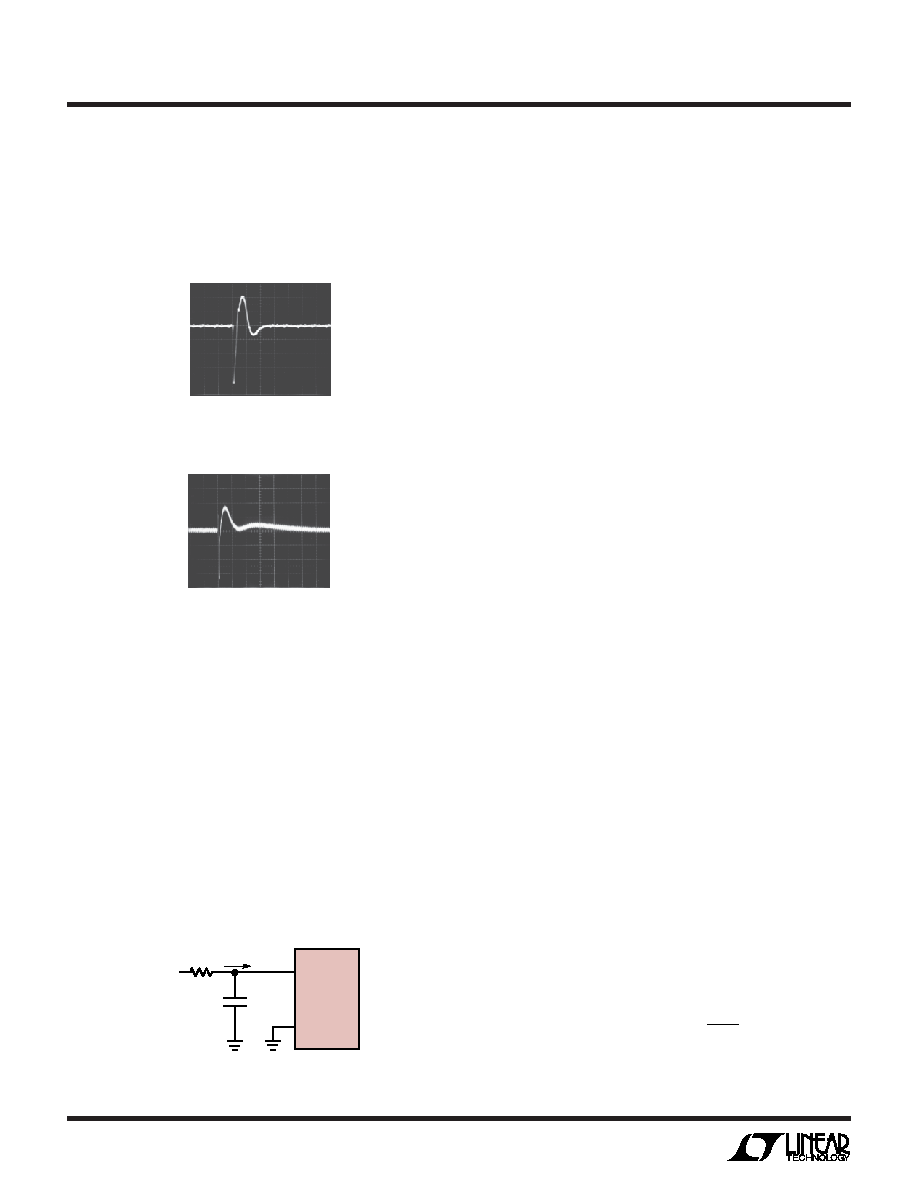
Figure 11. RC Input Filtering
RFILTER
VIN –
CFILTER
LTC1293 F11
LTC1293/4/6
"+"
"–"
IIDC
within the minimum settling windows of 2.5
s (“+” input)
and 1
s(“–” input) that occurs at the maximum clock rate
of 1MHz. Figures 9 and 10 show examples of adequate
and poor op amp settling.
RC Input Filtering
It is possible to filter the inputs with an RC network as
shown in Figure 11. For large values of CF (e.g., 1F) the
capacitive input switching currents are averaged into a net
DC current. A filter should be chosen with a small resistor
and large capacitor to prevent DC drops across the resis-
tor. The magnitude of the DC current is approximately IDC
= 100pF
× VIN/tCYC and is roughly proportional to VIN.
When running at the minimum cycle time of 21.5
s, the
input current equals 23
A at VIN= 5V. Here a filter resistor
of 5
will cause 0.1LSB of full-scale error. If a larger filter
resistor must be used, errors can be reduced by increasing
the cycle time as shown in the typical performance char-
acteristic curve Maximum Filter Resistor vs Cycle Time.
Input Leakage Current
Input leakage currents also can create errors if the source
resistance gets too large. For example, the maximum input
leakage specification of 1
A (at 125°C) flowing through a
source resistance of 1k
will cause a voltage drop of 1mV
or 0.8LSB. This error will be much reduced at lower
temperatures because leakage drops rapidly (see typical
performance characteristic curve Input Channel Leakage
Current vs Temperature).
SAMPLE AND HOLD
Single-Ended Input
The LTC1293/4/6 provides a built-in sample and hold
(S&H) function for all signals acquired in the single-ended
mode (COM pin grounded). The sample and hold allows
the LTC1293/4/6 to convert rapidly varying signals (see
typical performance characteristic curve of S&H Acquisi-
tion Time vs Source Resistance). The input voltage is
sampled during the tSMPL time as shown in Figure 8. The
sampling interval begins as the bit preceding the MSBF bit
is shifted in and continues until the falling edge of the PS
bit is received. On this falling edge the S&H goes into the
hold mode and the conversion begins.
Differential Input
With a differential input the A/D no longer converts a
single voltage but converts the difference between two
voltages. The voltage on the selected “+” input is sampled
and held and can be rapidly time varying. The voltage on
the “–” pin must remain constant and be free of noise and
ripple throughout the conversion time. Otherwise the
differencing operation will not be done accurately. The
conversion time is 12 CLK cycles. Therefore a change in
the –IN input voltage during this interval can cause con-
version errors. For a sinusoidal voltage on the –IN input
this error would be:
Where f(–) is the frequency of the “–” input voltage, VPEAK
is its peak amplitude and fCLK is the frequency of the CLK.
Vf
V
f
ERROR MAX
PEAK
CLK
()
(–)
= π
()
2
12
HORIZONTAL: 20
s/DIV
HORIZONTAL: 500ns/DIV
Figure 9. Adequate Settling of Op Amp Driving Analog Input
Figure 10. Poor Op Amp Settling Can Cause A/D Errors
VERTICAL:
5mV/DIV
VERTICAL:
5mV/DIV
相关PDF资料 |
PDF描述 |
|---|---|
| LTC1294CCJ | 8-CH 12-BIT SUCCESSIVE APPROXIMATION ADC, SERIAL ACCESS, CDIP20 |
| LTC1296BCJ | 8-CH 12-BIT SUCCESSIVE APPROXIMATION ADC, SERIAL ACCESS, CDIP20 |
| LTC1296CCJ | 8-CH 12-BIT SUCCESSIVE APPROXIMATION ADC, SERIAL ACCESS, CDIP20 |
| LTC1294DCJ | 8-CH 12-BIT SUCCESSIVE APPROXIMATION ADC, SERIAL ACCESS, CDIP20 |
| LTC1296DCJ | 8-CH 12-BIT SUCCESSIVE APPROXIMATION ADC, SERIAL ACCESS, CDIP20 |
相关代理商/技术参数 |
参数描述 |
|---|---|
| LTC1294BCN | 功能描述:IC DATA ACQ SYSTEM 12BIT 20-DIP RoHS:否 类别:集成电路 (IC) >> 数据采集 - ADCs/DAC - 专用型 系列:- 产品培训模块:Lead (SnPb) Finish for COTS Obsolescence Mitigation Program 标准包装:50 系列:- 类型:数据采集系统(DAS) 分辨率(位):16 b 采样率(每秒):21.94k 数据接口:MICROWIRE?,QSPI?,串行,SPI? 电压电源:模拟和数字 电源电压:1.8 V ~ 3.6 V 工作温度:-40°C ~ 85°C 安装类型:表面贴装 封装/外壳:40-WFQFN 裸露焊盘 供应商设备封装:40-TQFN-EP(6x6) 包装:托盘 |
| LTC1294BCN#PBF | 功能描述:IC DATA ACQ SYSTEM 12BIT 20-DIP RoHS:是 类别:集成电路 (IC) >> 数据采集 - ADCs/DAC - 专用型 系列:- 产品培训模块:Lead (SnPb) Finish for COTS Obsolescence Mitigation Program 标准包装:50 系列:- 类型:数据采集系统(DAS) 分辨率(位):16 b 采样率(每秒):21.94k 数据接口:MICROWIRE?,QSPI?,串行,SPI? 电压电源:模拟和数字 电源电压:1.8 V ~ 3.6 V 工作温度:-40°C ~ 85°C 安装类型:表面贴装 封装/外壳:40-WFQFN 裸露焊盘 供应商设备封装:40-TQFN-EP(6x6) 包装:托盘 |
| LTC1294BCSW | 功能描述:IC DATA ACQ SYSTEM 12BIT 20-SOIC RoHS:否 类别:集成电路 (IC) >> 数据采集 - ADCs/DAC - 专用型 系列:- 产品培训模块:Lead (SnPb) Finish for COTS Obsolescence Mitigation Program 标准包装:50 系列:- 类型:数据采集系统(DAS) 分辨率(位):16 b 采样率(每秒):21.94k 数据接口:MICROWIRE?,QSPI?,串行,SPI? 电压电源:模拟和数字 电源电压:1.8 V ~ 3.6 V 工作温度:-40°C ~ 85°C 安装类型:表面贴装 封装/外壳:40-WFQFN 裸露焊盘 供应商设备封装:40-TQFN-EP(6x6) 包装:托盘 |
| LTC1294BCSW#PBF | 功能描述:IC DATA ACQ SYSTEM 12BIT 20-SOIC RoHS:是 类别:集成电路 (IC) >> 数据采集 - ADCs/DAC - 专用型 系列:- 产品培训模块:Lead (SnPb) Finish for COTS Obsolescence Mitigation Program 标准包装:50 系列:- 类型:数据采集系统(DAS) 分辨率(位):16 b 采样率(每秒):21.94k 数据接口:MICROWIRE?,QSPI?,串行,SPI? 电压电源:模拟和数字 电源电压:1.8 V ~ 3.6 V 工作温度:-40°C ~ 85°C 安装类型:表面贴装 封装/外壳:40-WFQFN 裸露焊盘 供应商设备封装:40-TQFN-EP(6x6) 包装:托盘 |
| LTC1294BCSW#TR | 功能描述:IC DATA ACQ SYS 12BIT 5V 20SOIC RoHS:否 类别:集成电路 (IC) >> 数据采集 - ADCs/DAC - 专用型 系列:- 产品培训模块:Lead (SnPb) Finish for COTS Obsolescence Mitigation Program 标准包装:50 系列:- 类型:数据采集系统(DAS) 分辨率(位):16 b 采样率(每秒):21.94k 数据接口:MICROWIRE?,QSPI?,串行,SPI? 电压电源:模拟和数字 电源电压:1.8 V ~ 3.6 V 工作温度:-40°C ~ 85°C 安装类型:表面贴装 封装/外壳:40-WFQFN 裸露焊盘 供应商设备封装:40-TQFN-EP(6x6) 包装:托盘 |
发布紧急采购,3分钟左右您将得到回复。