- 您现在的位置:买卖IC网 > PDF目录1934 > LTC1343IGW#TRPBF (Linear Technology)IC TXRX SOFTWARE-SELECTBL 44SSOP PDF资料下载
参数资料
| 型号: | LTC1343IGW#TRPBF |
| 厂商: | Linear Technology |
| 文件页数: | 9/28页 |
| 文件大小: | 0K |
| 描述: | IC TXRX SOFTWARE-SELECTBL 44SSOP |
| 标准包装: | 1,000 |
| 类型: | 收发器 |
| 驱动器/接收器数: | 4/4 |
| 规程: | 多协议 |
| 电源电压: | 4.75 V ~ 5.25 V |
| 安装类型: | 表面贴装 |
| 封装/外壳: | 44-BSOP(0.295",7.50mm 宽) |
| 供应商设备封装: | 44-SSOP |
| 包装: | 带卷 (TR) |
第1页第2页第3页第4页第5页第6页第7页第8页当前第9页第10页第11页第12页第13页第14页第15页第16页第17页第18页第19页第20页第21页第22页第23页第24页第25页第26页第27页第28页
17
LTC1343
No-Cable Mode
The no-cable mode (M0 = M1 = M2 = 1) is intended for the
case when the cable is disconnected from the connector.
The charge pump, bias circuitry, drivers and receivers are
turned off, the driver outputs are forced into a high
impedance state, and the supply current drops to less than
200
A. It can also be used to share I/O lines with other
drivers and receivers without loading down the signals.
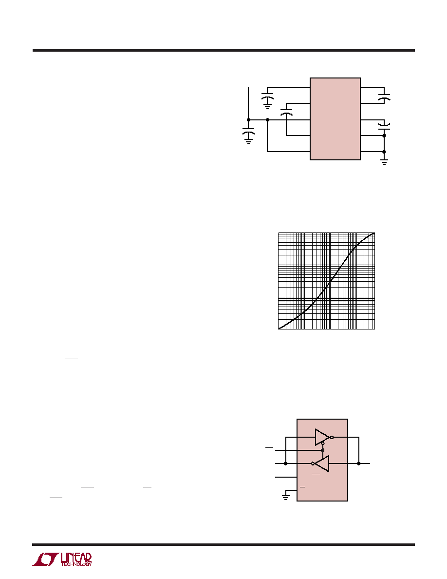
Charge Pump
The LTC1343 uses an internal capacitive charge pump to
generate VDD and VEE as shown in Figure 28. A voltage
doubler generates about 8V on VDD and a voltage inverter
generates about – 7.5V for VEE. Four 1F surface mounted
tantalum or ceramic capacitors are required for C1, C2, C3
and C4. The VEE capacitor C5 should be a minimum of
3.3
F. All capacitors are 16V.
Receiver Fail-Safe and Glitch Filter
All LTC1343 receivers feature fail-safe operation in all
modes except no-cable mode. If the receiver inputs are left
floating or shorted together by a termination resistor, the
receiver output will always be forced to a logic high.
External pull-up resistors are required on receiver outputs
if fail-safe operation in the no-cable mode is desired.
When the chip is configured for control signals by pulling
the CTRL/CLK pin high, a glitch filter is connected to all
receiver inputs. The filter will reject any glitches at the
receiver inputs less than 300ns.
V.10 Driver Rise and Fall Times
The rise and fall times of the V.10 drivers is programmed
by placing a 1/8W, 5% resistor between the 423 SET (Pin
25) and ground. The graph of Driver Rise and Fall Times
vs Resistor Value is shown in Figure 29.
Enabling the Single-Ended Driver and Receiver
When the LTC1343 is being used to generate the control
signals (CTRL/CLK = high) and the EC pin is pulled low, the
DCE/DTE pin becomes an enable for driver 1 and receiver
4 so their inputs and outputs can be tied together as shown
in Figure 30.
APPLICATIONS INFORMATION
WU
U
Figure 30. Single-Ended Driver and Receiver Enable
Figure 29. V.10 Driver Rise and Fall Time vs Resistor Value
Figure 28. Charge Pump
44
43
42
41
40
1343 F28
1
2
3
4
8
C3
1
F
C4
1
F
5V
C1
1
F
C2
1
F
C5
3.3
F
LTC1343
VDD
C1+
PWRVCC
C1–
VCC
C2+
C2–
VEE
PGND
GND
+
RESISTANCE (
)
DRIVER
RISE/FALL
TIME
(
s)
1k
100
10
1
0.1
100k
1M
5M
1343 F29
10k
39
26
LTC1343
1343 F30
5
21
16
20
24
EC
D1
CTRL/CLK
DCE/DTE
R4
VCC
相关PDF资料 |
PDF描述 |
|---|---|
| LTC1344AIG#TRPBF | IC CABLE TERM MULTIPROTCL 24SSOP |
| LTC1344CG | IC CABLE TERM MULTIPROTCL 24SSOP |
| LTC1345ISW#TRPBF | IC TXRX V.35 SINGL SUPPLY 28SOIC |
| LTC1346ACSW#TRPBF | IC TXRX V.35 DCE/DTE 24-SOIC |
| LTC1347CSW#TRPBF | IC TXRX 5V RS232 LOW PWR 28-SOIC |
相关代理商/技术参数 |
参数描述 |
|---|---|
| LTC1344ACG | 功能描述:IC CABLE TERM MULTIPROTCL 24SSOP RoHS:否 类别:集成电路 (IC) >> 接口 - 信号终端器 系列:- 产品培训模块:Lead (SnPb) Finish for COTS Obsolescence Mitigation Program 标准包装:50 系列:- 类型:SCSI,SE 端子数:9 电源电压:4 V ~ 5.25 V 工作温度:0°C ~ 70°C 安装类型:表面贴装 封装/外壳:16-SOIC(0.154",3.90mm 宽) 供应商设备封装:16-SOIC 包装:管件 |
| LTC1344ACG#PBF | 功能描述:IC CABLE TERM MULTIPROTCL 24SSOP RoHS:是 类别:集成电路 (IC) >> 接口 - 信号终端器 系列:- 产品培训模块:Lead (SnPb) Finish for COTS Obsolescence Mitigation Program 标准包装:50 系列:- 类型:SCSI,SE 端子数:9 电源电压:4 V ~ 5.25 V 工作温度:0°C ~ 70°C 安装类型:表面贴装 封装/外壳:16-SOIC(0.154",3.90mm 宽) 供应商设备封装:16-SOIC 包装:管件 |
| LTC1344ACG#TR | 功能描述:IC TERMINATOR CABLE MULTI 24SSOP RoHS:否 类别:集成电路 (IC) >> 接口 - 信号终端器 系列:- 产品培训模块:Lead (SnPb) Finish for COTS Obsolescence Mitigation Program 标准包装:50 系列:- 类型:SCSI,SE 端子数:9 电源电压:4 V ~ 5.25 V 工作温度:0°C ~ 70°C 安装类型:表面贴装 封装/外壳:16-SOIC(0.154",3.90mm 宽) 供应商设备封装:16-SOIC 包装:管件 |
| LTC1344ACG#TRPBF | 功能描述:IC CABLE TERM MULTIPROTCL 24SSOP RoHS:是 类别:集成电路 (IC) >> 接口 - 信号终端器 系列:- 产品培训模块:Lead (SnPb) Finish for COTS Obsolescence Mitigation Program 标准包装:50 系列:- 类型:SCSI,SE 端子数:9 电源电压:4 V ~ 5.25 V 工作温度:0°C ~ 70°C 安装类型:表面贴装 封装/外壳:16-SOIC(0.154",3.90mm 宽) 供应商设备封装:16-SOIC 包装:管件 |
| LTC1344AIG | 功能描述:IC TERMINATOR CABLE MULTI 24SSOP RoHS:否 类别:集成电路 (IC) >> 接口 - 信号终端器 系列:- 产品培训模块:Lead (SnPb) Finish for COTS Obsolescence Mitigation Program 标准包装:50 系列:- 类型:SCSI,SE 端子数:9 电源电压:4 V ~ 5.25 V 工作温度:0°C ~ 70°C 安装类型:表面贴装 封装/外壳:16-SOIC(0.154",3.90mm 宽) 供应商设备封装:16-SOIC 包装:管件 |
发布紧急采购,3分钟左右您将得到回复。