- 您现在的位置:买卖IC网 > PDF目录2003 > LTC1387IG#TRPBF (Linear Technology)IC TXRX RS232/RS485 5VSNGL20SSOP PDF资料下载
参数资料
| 型号: | LTC1387IG#TRPBF |
| 厂商: | Linear Technology |
| 文件页数: | 7/12页 |
| 文件大小: | 0K |
| 描述: | IC TXRX RS232/RS485 5VSNGL20SSOP |
| 标准包装: | 1,800 |
| 类型: | 收发器 |
| 驱动器/接收器数: | 2/2 |
| 规程: | RS232,RS485 |
| 电源电压: | 5V |
| 安装类型: | 表面贴装 |
| 封装/外壳: | 20-SSOP(0.209",5.30mm 宽) |
| 供应商设备封装: | 20-SSOP |
| 包装: | 带卷 (TR) |
4
LTC1387
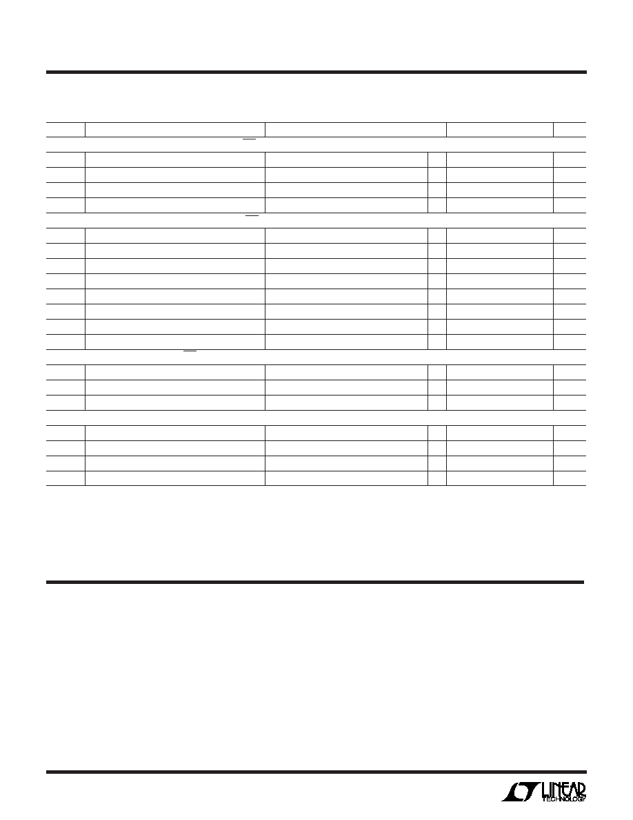
AC ELECTRICAL CHARACTERISTICS
TA = 25°C, VCC = 5V, C1 = C2 = C3 = C4 = 0.1F (Notes 2, 3), unless otherwise noted.
The q denotes specifications which apply over the full operating
temperature range.
Note 1: Absolute Maximum Ratings are those values beyond which the life
of the device may be impaired.
Note 2: All currents into device pins are positive; all currents out of device
pins are negative. All voltages are referenced to device ground unless
otherwise specified.
Note 3: All typicals are given at VCC = 5V, C1 = C2 = C3 = C4 = 0.1F
and TA = 25°C.
Note 4: Short-circuit current for RS485 driver output low state folds back
above VCC. Peak current occurs around VO = 3V.
Note 5: SLEW includes an internal pull-up in RS485 mode.
PIN FUNCTIONS
UU
U
C1+ (Pin 1): Commutating Capacitor C1 Positive Terminal.
Requires an external 0.1
F capacitor between Pins 1 and 2.
C1– (Pin 2): Commutating Capacitor C1 Negative Terminal.
VDD (Pin 3): Charge Pump Positive Supply Output.
Requires an external 0.1
F capacitor to ground.
A (Pin 4): Receiver Input A. Inverting input of RS232
receiver A in RS232 mode; inverting RS485 receiver input
in RS485 mode.
B (Pin 5): Receiver Input B. Inverting input of RS232
receiver B in RS232 mode; noninverting RS485 receiver
input in RS485 mode.
Y (Pin 6): Driver Output Y. Inverting RS232 driver Y output
in RS232 mode; inverting RS485 driver output in RS485
mode.
Z (Pin 7): Driver Output Z. Inverting RS232 driver Z output
in RS232 mode; noninverting RS485 driver output in
RS485 mode.
SYMBOL
PARAMETER
CONDITIONS
MIN
TYP
MAX
UNITS
RS485 Mode (Fast Slew Rate, ON = DXEN = High, 485/232 = High, SLEW = High)
tZL
Driver Enable to Output Low
Figures 3, 8, CL = 100pF, S1 Closed
q
50
90
ns
tZH
Driver Enable to Output High
Figures 3, 8, CL = 100pF, S2 Closed
q
50
90
ns
tLZ
Driver Disable from Low
Figures 3, 8, CL = 15pF, S1 Closed
q
50
90
ns
tHZ
Driver Disable from High
Figures 3, 8, CL = 15pF, S2 Closed
q
60
90
ns
RS485 Mode (Slow Slew Rate, ON = DXEN = High, 485/232 = High, SLEW = Low)
tPLH
Driver Input to Output
Figures 2, 7, RL = 54, CL = 100pF
q
100
700
1500
ns
tPHL
Driver Input to Output
Figures 2, 7, RL = 54, CL = 100pF
q
100
700
1500
ns
tSKEW
Driver Output to Output
Figures 2, 7, RL = 54, CL = 100pF
q
200
750
ns
tr, tf
Driver Rise or Fall Time
Figures 2, 7, RL = 54, CL = 100pF
q
150
300
1500
ns
tZL
Driver Enable to Output Low
Figures 3, 8, CL = 100pF, S1 Closed
q
600
1500
ns
tZH
Driver Enable to Output High
Figures 3, 8, CL = 100pF, S2 Closed
q
600
1500
ns
tLZ
Driver Disable from Low
Figures 3, 8, CL = 15pF, S1 Closed
q
100
200
ns
tHZ
Driver Disable from High
Figures 3, 8, CL = 15pF, S2 Closed
q
100
200
ns
RS485 Mode (ON = RXEN = High, 485/232 = High)
tPLH
Receiver Input to Output
Figures 2, 9, RL = 54, CL = 100pF
q
20
70
140
ns
tPHL
Receiver Input to Output
Figures 2, 9, RL = 54, CL = 100pF
q
20
70
140
ns
tSKEW
Differential Receiver Skew,
tPLH – tPHL
Figures 2, 9, RL = 54, CL = 100pF
10
ns
Receiver Output Enable/Disable (ON = High)
tZL
Receiver Enable to Output Low
Figures 6, 12, CL = 15pF, S1 Closed
q
40
90
ns
tZH
Receiver Enable to Output High
Figures 6, 12, CL = 15pF, S2 Closed
q
40
90
ns
tLZ
Receiver Disable from Low
Figures 6, 12, CL = 15pF, S1 Closed
q
40
90
ns
tHZ
Receiver Disable from High
Figures 6, 12, CL = 15pF, S2 Closed
q
40
90
ns
相关PDF资料 |
PDF描述 |
|---|---|
| LTC1400IS8 | IC A/D CONV 12BIT W/SHTDN 8-SOIC |
| LTC1401IS8#TRPBF | IC A/D CONV 12BIT W/SHTDN 8-SOIC |
| LTC1402IGN#TRPBF | IC ADC 12BIT 2.2MSPS SHDN 16SSOP |
| LTC1403AHMSE#TRPBF | IC ADC 14BIT 2.8MSPS DIFF 10MSOP |
| LTC1403AIMSE-1#TRPBF | IC ADC 14BIT 2.8MSPS DIFF 10MSOP |
相关代理商/技术参数 |
参数描述 |
|---|---|
| LTC1387ISW | 制造商:Linear Technology 功能描述:Single Transmitter/Receiver RS-232/RS-485 20-Pin SOIC W |
| LTC1387ISW#PBF | 功能描述:IC TXRX RS232/RS485 5VSNGL20SOIC RoHS:是 类别:集成电路 (IC) >> 接口 - 驱动器,接收器,收发器 系列:- 产品培训模块:RS-232 & USB Transceiver 标准包装:2,000 系列:- 类型:收发器 驱动器/接收器数:1/1 规程:RS232 电源电压:3 V ~ 5.5 V 安装类型:表面贴装 封装/外壳:16-SSOP(0.209",5.30mm 宽) 供应商设备封装:16-SSOP 包装:带卷 (TR) 其它名称:296-19849-2 |
| LTC1387ISW#TR | 功能描述:IC TXRX RS232/RS485 5V 20SOIC RoHS:否 类别:集成电路 (IC) >> 接口 - 驱动器,接收器,收发器 系列:- 标准包装:27 系列:- 类型:收发器 驱动器/接收器数:3/3 规程:RS232,RS485 电源电压:4.75 V ~ 5.25 V 安装类型:表面贴装 封装/外壳:28-SOIC(0.295",7.50mm 宽) 供应商设备封装:28-SOIC 包装:管件 |
| LTC1387ISW#TRPBF | 功能描述:IC TXRX RS232/RS485 5VSNGL20SOIC RoHS:是 类别:集成电路 (IC) >> 接口 - 驱动器,接收器,收发器 系列:- 标准包装:27 系列:- 类型:收发器 驱动器/接收器数:3/3 规程:RS232,RS485 电源电压:4.75 V ~ 5.25 V 安装类型:表面贴装 封装/外壳:28-SOIC(0.295",7.50mm 宽) 供应商设备封装:28-SOIC 包装:管件 |
| LTC1387ISWPBF | 制造商:Linear Technology 功能描述:RS-232/RS-485 Driver/Receiver SOIC20W |
发布紧急采购,3分钟左右您将得到回复。