- 您现在的位置:买卖IC网 > PDF目录2003 > LTC1401IS8#TRPBF (Linear Technology)IC A/D CONV 12BIT W/SHTDN 8-SOIC PDF资料下载
参数资料
| 型号: | LTC1401IS8#TRPBF |
| 厂商: | Linear Technology |
| 文件页数: | 3/20页 |
| 文件大小: | 0K |
| 描述: | IC A/D CONV 12BIT W/SHTDN 8-SOIC |
| 标准包装: | 2,500 |
| 位数: | 12 |
| 采样率(每秒): | 200k |
| 数据接口: | MICROWIRE?,串行,SPI? |
| 转换器数目: | 1 |
| 功率耗散(最大): | 30mW |
| 电压电源: | 单电源 |
| 工作温度: | -40°C ~ 85°C |
| 安装类型: | 表面贴装 |
| 封装/外壳: | 8-SOIC(0.154",3.90mm 宽) |
| 供应商设备封装: | 8-SOIC |
| 包装: | 带卷 (TR) |
| 输入数目和类型: | 1 个单端,单极 |
11
LTC1401
1401fa
APPLICATIONS INFORMATION
WU
U
BOARD LAYOUT AND BYPASSING
Wire wrap boards are not recommended for high resolu-
tion or high speed A/D converters. To obtain the best
performance from the LTC1401, a printed circuit board is
required. Layout for the printed circuit board should
ensure that digital and analog signal lines are separated as
much as possible. In particular, care should be taken not
to run any digital traces alongside an analog signal trace
or underneath the ADC. The analog input should be
screened by GND.
High quality tantalum and ceramic bypass capacitors
should be used at the VCC and VREF pins as shown in the
Typical Application on the first page of this datasheet. For
LTC1401 F09b
–
+
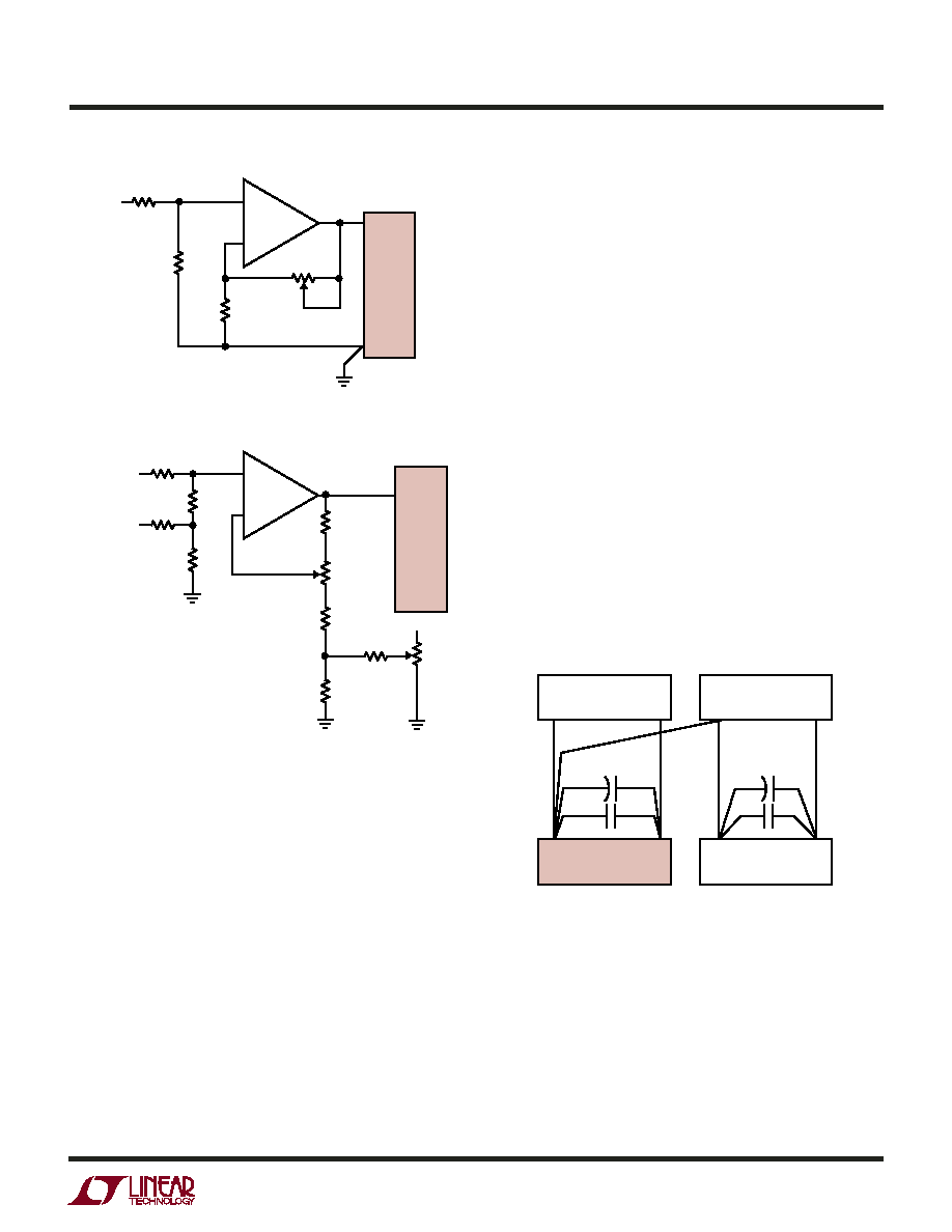
R2
10k
R9
20
R4
100k
R5
4.3k
FULL-SCALE
ADJUST
R3
100k
R6
400
R1
10k
ANALOG
INPUT
0V TO 2.048V
A1
3V
R8
10k
OFFSET
ADJUST
R7
100k
3V
AIN
LTC1401
optimum performance, a 10
F surface mount AVX capaci-
tor in parallel with a 0.1
Fceramicisrecommendedforthe
VCC and VREF pins. The capacitors must be located as close
to the pins as possible. The traces connecting the pins and
the bypass capacitors must be kept short and should be
made as wide as possible.
Input signal leads to AIN and signal return leads from GND
(Pin 4) should be kept as short as possible to minimize
noise coupling. In applications where this is not possible,
a shielded cable between the analog input signal and the
ADC is recommended. Also, any potential difference in
grounds between the analog signal and the ADC appears
as an error voltage in series with the analog input signal.
Attention should be paid to reducing the ground circuit
impedance as much as possible.
Figure 10 shows the recommended system ground con-
nections. All analog circuitry grounds should be termi-
nated at the LTC1401 GND pin. The ground return to the
power supply from Pin 4 should be low impedance for
noise free operation. Digital circuitry grounds must be
connected to the digital supply common.
Figure 9a. LTC1401 Full-Scale Adjust Circuit
LTC1401 F09a
–
+
R2
10k
R3
10k
R1
50
R4
100
FULL-SCALE
ADJUST
VIN
A1
LTC1401
AIN
GND
ADDITIONAL PINS OMITTED FOR CLARITY
±20LSB TRIM RANGE
Figure 9b. LTC1401 Offset and Full-Scale Adjust Circuit
Figure 10. Power Supply Connection
ANALOG SUPPLY
GND
3V
+
LTC1401
VCC
GND
DIGITAL SUPPLY
GND
3V
+
DIGITAL CIRCUITRY
VCC
GND
LTC1401 F10
Power-Down Mode
Upon power up, the LTC1401 is initialized to the active
state and is ready for conversion. However, the chip can be
easily placed into Nap or Sleep mode by exercising the
right combination of CLK and CONV signals. In Nap mode,
all power is off except the internal reference which remains
active and provides 1.20V output voltage to the other
相关PDF资料 |
PDF描述 |
|---|---|
| LTC1402IGN#TRPBF | IC ADC 12BIT 2.2MSPS SHDN 16SSOP |
| LTC1403AHMSE#TRPBF | IC ADC 14BIT 2.8MSPS DIFF 10MSOP |
| LTC1403AIMSE-1#TRPBF | IC ADC 14BIT 2.8MSPS DIFF 10MSOP |
| LTC1404IS8#TRPBF | IC A/D CONV 12BIT W/SHTDN 8-SOIC |
| LTC1405IGN#TRPBF | IC ADC 12BIT 5MSPS SAMPLE 28SSOP |
相关代理商/技术参数 |
参数描述 |
|---|---|
| LTC1402CGN | 功能描述:IC ADC 12BIT 2.2MSPS SHDN 16SSOP RoHS:否 类别:集成电路 (IC) >> 数据采集 - 模数转换器 系列:- 标准包装:1,000 系列:- 位数:16 采样率(每秒):45k 数据接口:串行 转换器数目:2 功率耗散(最大):315mW 电压电源:模拟和数字 工作温度:0°C ~ 70°C 安装类型:表面贴装 封装/外壳:28-SOIC(0.295",7.50mm 宽) 供应商设备封装:28-SOIC W 包装:带卷 (TR) 输入数目和类型:2 个单端,单极 |
| LTC1402CGN#PBF | 功能描述:IC ADC 12BIT 2.2MSPS SHDN 16SSOP RoHS:是 类别:集成电路 (IC) >> 数据采集 - 模数转换器 系列:- 标准包装:1 系列:microPOWER™ 位数:8 采样率(每秒):1M 数据接口:串行,SPI? 转换器数目:1 功率耗散(最大):- 电压电源:模拟和数字 工作温度:-40°C ~ 125°C 安装类型:表面贴装 封装/外壳:24-VFQFN 裸露焊盘 供应商设备封装:24-VQFN 裸露焊盘(4x4) 包装:Digi-Reel® 输入数目和类型:8 个单端,单极 产品目录页面:892 (CN2011-ZH PDF) 其它名称:296-25851-6 |
| LTC1402CGN#TR | 功能描述:IC ADC 12BIT 2.2MSPS SHDN 16SSOP RoHS:否 类别:集成电路 (IC) >> 数据采集 - 模数转换器 系列:- 标准包装:1,000 系列:- 位数:16 采样率(每秒):45k 数据接口:串行 转换器数目:2 功率耗散(最大):315mW 电压电源:模拟和数字 工作温度:0°C ~ 70°C 安装类型:表面贴装 封装/外壳:28-SOIC(0.295",7.50mm 宽) 供应商设备封装:28-SOIC W 包装:带卷 (TR) 输入数目和类型:2 个单端,单极 |
| LTC1402CGN#TRPBF | 功能描述:IC ADC 12BIT 2.2MSPS SHDN 16SSOP RoHS:是 类别:集成电路 (IC) >> 数据采集 - 模数转换器 系列:- 标准包装:1,000 系列:- 位数:16 采样率(每秒):45k 数据接口:串行 转换器数目:2 功率耗散(最大):315mW 电压电源:模拟和数字 工作温度:0°C ~ 70°C 安装类型:表面贴装 封装/外壳:28-SOIC(0.295",7.50mm 宽) 供应商设备封装:28-SOIC W 包装:带卷 (TR) 输入数目和类型:2 个单端,单极 |
| LTC1402CGNPBF | 制造商:Linear Technology 功能描述:ADC,LTC1402 12bit 2.2MSPS SPI SSOP |
发布紧急采购,3分钟左右您将得到回复。