- 您现在的位置:买卖IC网 > PDF目录10679 > LTC1403IMSE#PBF (Linear Technology)IC ADC 12BIT 2.8MSPS 10-MSOP PDF资料下载
参数资料
| 型号: | LTC1403IMSE#PBF |
| 厂商: | Linear Technology |
| 文件页数: | 4/20页 |
| 文件大小: | 0K |
| 描述: | IC ADC 12BIT 2.8MSPS 10-MSOP |
| 标准包装: | 50 |
| 位数: | 12 |
| 采样率(每秒): | 2.8M |
| 数据接口: | 串行,SPI? |
| 转换器数目: | 1 |
| 功率耗散(最大): | 12mW |
| 电压电源: | 单电源 |
| 工作温度: | -40°C ~ 85°C |
| 安装类型: | 表面贴装 |
| 封装/外壳: | 10-TFSOP,10-MSOP(0.118",3.00mm 宽)裸露焊盘 |
| 供应商设备封装: | 10-MSOP 裸露焊盘 |
| 包装: | 管件 |
| 输入数目和类型: | 2 个单端,单极;1 个差分,单极 |
| 产品目录页面: | 1346 (CN2011-ZH PDF) |
| 配用: | DC1082A-D-ND - BOARD SAR ADC LTC1403A DC1082A-C-ND - BOARD SAR ADC LTC1403A-1 |
LTC1403/LTC1403A
12
1403fb
APPLICATIONS INFORMATION
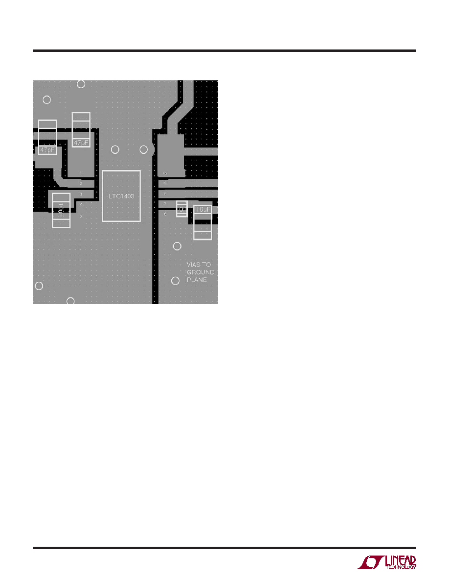
Board Layout and Bypassing
Wire wrap boards are not recommended for high resolu-
tion and/or high speed A/D converters. To obtain the best
performance from the LTC1403/LTC1403A, a printed circuit
board with ground plane is required. Layout for the printed
circuit board should ensure that digital and analog signal
lines are separated as much as possible. In particular, care
should be taken not to run any digital track alongside an
analog signal track. If optimum phase match between the
inputs is desired, the length of the two input wires should
be kept matched.
High quality tantalum and ceramic bypass capacitors
should be used at the VDD and VREF pins as shown in
the Block Diagram on the rst page of this data sheet.
For optimum performance, a 10μF surface mount AVX
capacitor with a 0.1μF ceramic is recommended for
the VDD and VREF pins. Alternatively, 10μF ceramic chip
capacitors such as Murata GRM235Y5V106Z016 may
be used. The capacitors must be located as close to the
pins as possible. The traces connecting the pins and the
bypass capacitors must be kept short and should be made
as wide as possible.
Figure 5 shows the recommended system ground connec-
tions. All analog circuitry grounds should be terminated
at the LTC1403/LTC1403A GND (Pins 4, 5, 6 and exposed
pad). The ground return from the LTC1403/LTC1403A (Pins
4, 5, 6 and exposed pad) to the power supply should be
low impedance for noise free operation. Digital circuitry
grounds must be connected to the digital supply com-
mon. In applications where the ADC data outputs and
control signals are connected to a continuously active
microprocessor bus, it is possible to get errors in the
conversion results. These errors are due to feedthrough
from the microprocessor to the successive approximation
comparator. The problem can be eliminated by forcing the
microprocessor into a Wait state during conversion or by
using three-state buffers to isolate the ADC data bus.
POWER-DOWN MODES
Upon power-up, the LTC1403/LTC1403A is initialized to
the active state and is ready for conversion. The Nap and
Sleep mode waveforms show the power-down modes for
the LTC1403/LTC1403A. The SCK and CONV inputs control
the power-down modes (see Timing Diagrams). Two rising
edges at CONV, without any intervening rising edges at SCK,
put the LTC1403/LTC1403A in Nap mode and the power
drain drops from 14mW to 6mW. The internal reference
remains powered in Nap mode. One or more rising edges
at SCK wake up the LTC1403/LTC1403A for service very
quickly, and CONV can start an accurate conversion within
a clock cycle. Four rising edges at CONV, without any
Figure 5. Recommended Layout
相关PDF资料 |
PDF描述 |
|---|---|
| VE-JWK-MY-F2 | CONVERTER MOD DC/DC 40V 50W |
| VI-B2N-MY-B1 | CONVERTER MOD DC/DC 18.5V 50W |
| LTC1407IMSE-1#PBF | IC ADC 12BIT 3MSPS 10-MSOP |
| LT6700MPDCB-1#TRMPBF | IC COMP DUAL 400MV REF 6-DFN |
| VE-JWK-MY-F1 | CONVERTER MOD DC/DC 40V 50W |
相关代理商/技术参数 |
参数描述 |
|---|---|
| LTC1404CS8 | 功能描述:IC A/D CONV 12BIT W/SHTDN 8-SOIC RoHS:否 类别:集成电路 (IC) >> 数据采集 - 模数转换器 系列:- 标准包装:1,000 系列:- 位数:16 采样率(每秒):45k 数据接口:串行 转换器数目:2 功率耗散(最大):315mW 电压电源:模拟和数字 工作温度:0°C ~ 70°C 安装类型:表面贴装 封装/外壳:28-SOIC(0.295",7.50mm 宽) 供应商设备封装:28-SOIC W 包装:带卷 (TR) 输入数目和类型:2 个单端,单极 |
| LTC1404CS8#PBF | 功能描述:IC A/D CONV 12BIT W/SHTDN 8-SOIC RoHS:是 类别:集成电路 (IC) >> 数据采集 - 模数转换器 系列:- 标准包装:1 系列:microPOWER™ 位数:8 采样率(每秒):1M 数据接口:串行,SPI? 转换器数目:1 功率耗散(最大):- 电压电源:模拟和数字 工作温度:-40°C ~ 125°C 安装类型:表面贴装 封装/外壳:24-VFQFN 裸露焊盘 供应商设备封装:24-VQFN 裸露焊盘(4x4) 包装:Digi-Reel® 输入数目和类型:8 个单端,单极 产品目录页面:892 (CN2011-ZH PDF) 其它名称:296-25851-6 |
| LTC1404CS8#TR | 功能描述:IC ADC 12BIT 600KSPS SHTDN 8SOIC RoHS:否 类别:集成电路 (IC) >> 数据采集 - 模数转换器 系列:- 标准包装:1,000 系列:- 位数:16 采样率(每秒):45k 数据接口:串行 转换器数目:2 功率耗散(最大):315mW 电压电源:模拟和数字 工作温度:0°C ~ 70°C 安装类型:表面贴装 封装/外壳:28-SOIC(0.295",7.50mm 宽) 供应商设备封装:28-SOIC W 包装:带卷 (TR) 输入数目和类型:2 个单端,单极 |
| LTC1404CS8#TRPBF | 功能描述:IC A/D CONV 12BIT W/SHTDN 8-SOIC RoHS:是 类别:集成电路 (IC) >> 数据采集 - 模数转换器 系列:- 标准包装:1,000 系列:- 位数:16 采样率(每秒):45k 数据接口:串行 转换器数目:2 功率耗散(最大):315mW 电压电源:模拟和数字 工作温度:0°C ~ 70°C 安装类型:表面贴装 封装/外壳:28-SOIC(0.295",7.50mm 宽) 供应商设备封装:28-SOIC W 包装:带卷 (TR) 输入数目和类型:2 个单端,单极 |
| LTC1404CS8PBF | 制造商:Linear Technology 功能描述:ADC,LTC1404 12bit 600kSPS SOIC |
发布紧急采购,3分钟左右您将得到回复。